This thread has been locked.

If you have a related question, please click the "Ask a related question" button in the top right corner. The newly created question will be automatically linked to this question.

ADS8344 failure modes

Other Parts Discussed in Thread: ADS8344

Hi,

I have encountered the case of an ADS8344NB sourcing seemingly too much current. The symptom was that the 5V supply sourced by a linear regulator was collapsing until I  disconnected pins 10, 11, 12 and 20 of the ADS8344 where this voltage was tied.

Is there any knowledge base about the way an ADS8344 could fail this way?

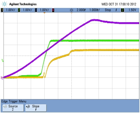
Our first analyse led to suspect a voltage measure on an analog input (pin 6) which grows half a millisecond before the converter 5V supply, thus exceeding the max rating (Vcc+0.3V).

On this plot : blue trace = ADS8344 +Vcc ; green trace = analog channel 5 input (pin6), every channels are used in single-ended mode.

This could habe been repeated roughly 30-50 times in the device's life.

Could it be the reason of the failure?

Thanks for any comment,

Best Regards,

Eric.

  • Hi Eric,

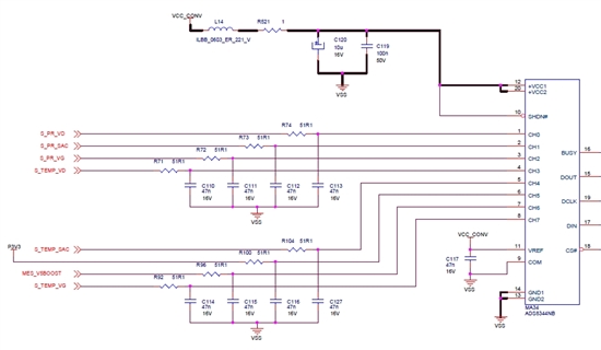
    I'm assuming you still have the same schematic as the one you provided in connection with your previous post ("ADS8344 first conversion"). The schematic does not show how CH5 is being driven, however based on what it does show, I believe that it is the VREF signal (pin 11) that is overloading your power supply (VCC_CONV).

    Immediately after you apply power to VCC_CONV, VREF quickly charges up to the supply voltage. On the other hand, the power supply for the chip, +VCC (pins 12, 20), ramps up at a much slower rate because of the extensive low-pass filtering you have on it. Since VREF is much greater than VCC, the ESD protection diode between VREF and VCC becomes forward-biased. This causes the VCC_CONV supply to current limit and collapse.

    I'd like to suggest a few changes for you to try:
    - Short the terminals of L14
    - Short the terminals of R521

    Please let me know how the changes work out for you.

    Best Regards,
    Harsha

  • Hi Harsha,

    Thanks for your answer which pointed the difference of voltage ramp-up speed between VREF and VCC pins. So, we have two overloading possibilities at power-up through ESD diodes : VREF and CH5.

    Here is a less zoomed version of the schematic :

    As you can see, CH5 is a 3.3V supply measured for test purposes. This is the green trace in my previous post. P3V3 and VCC_CONV are both sourced by the same 12V supply, but due to the filtering on VCC_CONV, it growths slowly compared to P3V3.

    But as VREF is now pointed to be overloaded as well, not only one channel, is damaging the entire ADC at power-up more believable?

    We only have one ADS8344 confirmed to be destroyed, among more than 30 healthy ones. I'll try to observe the VREF ramp-up to evaluate its overloading.

    I suggest to correct the schematic by connecting the VREF pin after the filter instead of shorting it.

    Best regards,

    Eric.

  • Hi Eric,

    I apologize for not replying earlier. I am presently on business travel, and unfortunately my responses have been a bit slow.

    Thank you for providing the additional schematic details. Yes, it appears that CH5 is overloading the supply but the 51ohm series resistor (R100) helps prevent ESD damage by limiting the forward current through the diode. On the other hand, there is no such mechanism on the VREF path to limit the ESD current. I suspect that repeatedly exercising the part in this fashion causes the protection circuitry to degrade and eventually the part fails.

    Yes, please try out the modification you have suggested and let me know what you find out. Thank you.

    Best Regards,
    Harsha

  • Hi Harsha,

    Don't worry about the delay between my last message and your answer.

    Thanks for your opinion about the VREF ESD diode, however I checked the voltage ramp at power-up on this pin, and it appears to be exactly the same as the filtered VCC_CONV on pins 12 and 20. I did not check if it is due to a slow ramp on VCC_CONV thanks to the capacitors on the regulator output, or even a slow P12V turn-on time on the regulator input.

    I'll let you know further investigations.

    Best regards,

    Eric.