This thread has been locked.

If you have a related question, please click the "Ask a related question" button in the top right corner. The newly created question will be automatically linked to this question.

Clocking Speed of ADS41B49 EVM

Other Parts Discussed in Thread: ADS41B49, ADS41B49EVM, ADS4249

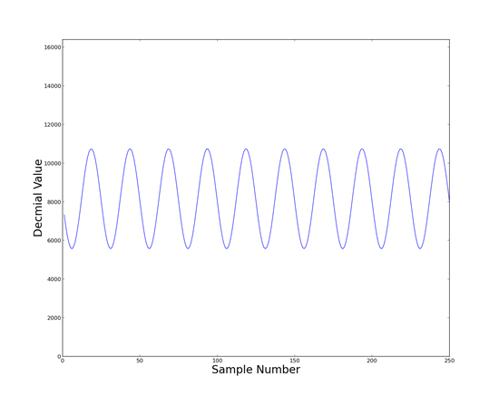
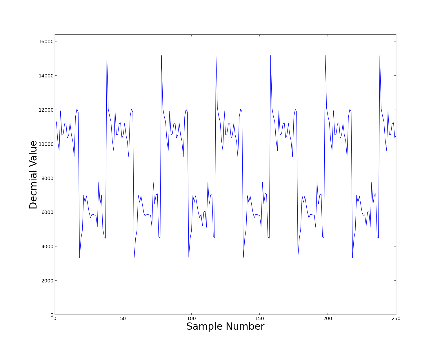
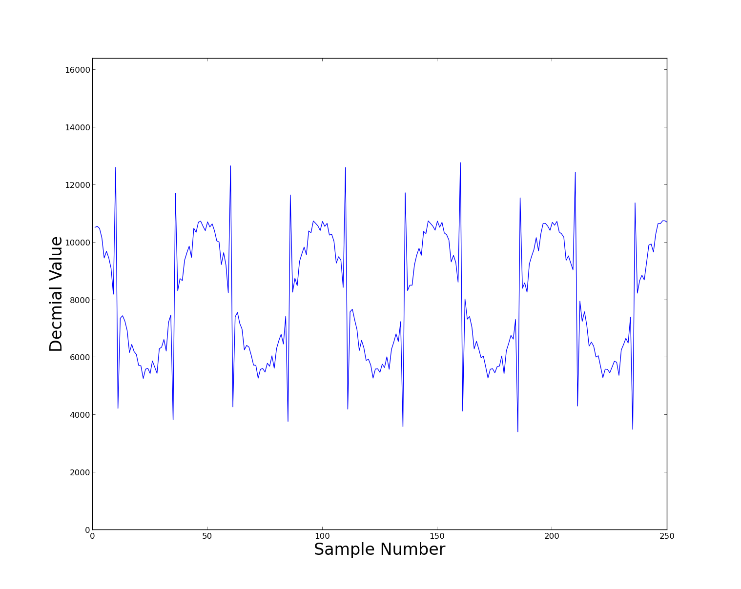
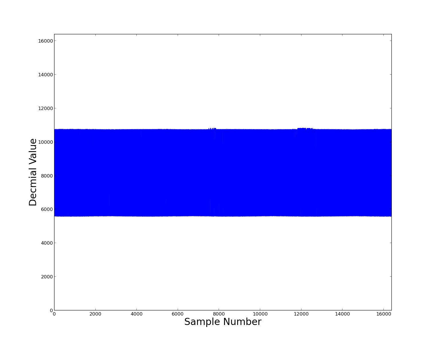
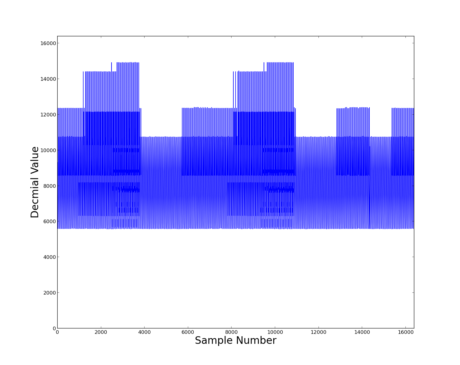
We are working with a ADS41B49 EVM and are trying to understand what is meant by a clocking speed of 250 MSPS.  When we provide a 250 MHz clock the data from the ADC is very spiky and wrong.  When we provide a 125 MHz clock the data from the ADC is exactly what we expect.  I have tested and anything above 125 MHz (even 126 MHz) is problematic.  If you would like some data to see for yourself I can send you some.

Thanks,

Kyle

  • Kyle,

    The clocking speed refers to the clock provided to the clock input. This is the "sampling rate" of the ADC. The ADS41B49 can sample up to 250 MSPS (Milliion samples per second). So, the ADS41B49 should be able to handle a clock speed of 250 MHz.

    Are you using the TI EVMs (ADS41B49EVM and TSW1400 or TSW1405) or your own board? Please send plots if you have them.

    Regards,
    Matt Guibord 

  • Thanks for the reply Matt,

    We are using a Cyclone V board with VHDL code modelled after http://www.ti.com/analog/docs/litabsmultiplefilelist.tsp?literatureNumber=slaa545&docCategoryId=1&familyId=390.  Here are a few plots showing what the results look like.

    125MHzCLK-5MHzSignal-1VP-P

    200MHzCLK-5MHzSignal-1VP-P


    250MHzCLK-5MHzSignal-1VP-P

    For a 125 MHz clock the results are exactly what we expect.  However, the tests of the clock at 200MHz and 250MHz show a lot of "noisy" (not really sure what the best name for it it) behavior.  Even clocking at 126MHz presents problems if you look at long enough times (Some incorrect values around samples 7000 and 12000).  You can see 126MHz and 125MHz clocks speeds below.

    125MHzCLK-5MHzSignal-1VP-P-Long

    126MHzCLK-5MHzSignal-1VP-P_Long

    I am new to this field so there is a good chance that I am doing something incorrect.  Open to suggestions and questions.

    Cheers,

    Kyle

  • Hi Kyle,

    Quick question. What is the amplitude of the clock you're providing to the ADC? Is it coming from your FPGA?

    This seems like it is possibly a timing problem. Are you using the ADC output clock to capture the data or are you using a separate clock? Do you have a schematic or block diagram I could see?

    Thanks,
    Matt Guibord 

  • The clock is provided by the FPGA.  At 125MHz it is ~.8V P-P.  At 250MHz it is ~.5V P-P.  The data-sheet does say that .7 VP-P is the typical input required for an LVDS clock so there is a chance that this is too small of a clock voltage.

  • I played around with the settings on the FPGA and now can get a 1V P-P clock out but the output still looks strange.  Parts of it have incorrect (spiky) readings while other portions are correct. 

    Here is the full sample.

    Zoomed In

    Any suggestions?

    Cheers,

    Kyle

  • Kyle,

    This is looking like a timing problem. Please answer my questions from the previous post:

    This seems like it is possibly a timing problem. Are you using the ADC output clock to capture the data or are you using a separate clock? Do you have a schematic or block diagram I could see?

    Regards,
    Matt Guibord 

  • Sorry, I was not quite sure what you were asking.  We use the ADC output clock fed into a source synchronous pll and use the clock provided by the pll to put the data into memory.  Here is a block diagram of the setup we are using right now.

    1715.Updated Sketch.docx

  • Kyle,

    Okay, so this should be very similar to the example project that you mentioned. Is your source-synchronous PLL adjusting the phase of the data clock or have you set it to 0 degrees?

    Second, have you implemented the timing constraints in your project? The constraints should essentially be the same for the ADS41B49 as they were for the ADS4249.

    Regards,
    Matt Guibord 

  • Matt,

    The source-synchronous PLL is set to 0 degrees.  I have not set any timing constraints.  I see that this is covered in 2.3 of the example project guide, I will read and try to implement that in my project.

    Cheers,

    Kyle

  • The issue is that quartus cannot find a way to fit the design in the FPGA and preserve signals of more than ~200 MHz.  We have changed our design to work within these limits and the problem seems to have been solved.

    Thanks for your time,

    Kyle