This thread has been locked.

If you have a related question, please click the "Ask a related question" button in the top right corner. The newly created question will be automatically linked to this question.

DAC8728 latching and power-up sequencing

Other Parts Discussed in Thread: DAC8728, ADS8555

Hi,

On page 41 of the DAC8728 it talks about the power sequencing. Since usually a 5V regulator is fed from +15V, and perhaps 3.3V regulator fed from the 5V or 15V, the power up sequencing is really backwards. Do you have any circuit proposals that will help with the sequencing? Are there any FET Switch type products that will help in this regard?

Also on Page 41, the datasheet indicates that "The DAC8728 permanently latches the status of some of the digital pins at power-on" and goes onto alude that these pins are "LDAC, CLR, RST, CS and RSTSEL". I could understand how and why RSTSEL would be latched, but not the others. Also, when looking for LDAC, CLR, RST and CS in the datasheet, the pin descriptions are rather ordinary, and nowhere else in the datasheet does it discuss that the state of these pins are latched or any other latching reference. 

Could you please provide more information about the "latching", what it is that is latched, why it is latched, etc.?

Thank you,
Marc 

  • Could someone help answering this question please...

  • Hi Marc,

    Sorry for the delays, I've been traveling a lot this month and haven't had the chance to really sit down to look at this problem.

    I agree that the power supply sequence is a little backwards from the perspective of typical power supply generation. In terms of typical power supply sequencing for mixed signal devices this is actually pretty normal, though. The reason for this sequencing is that the digital blocks power OTP memory internal to the device that contains important information like internal trim values. This information is used once the analog supplies are brought up to set various switches to meet the analog performance parameters specified in the datasheet. So, when you violate power supply sequences the device will most likely not be damaged but you may observe degraded or otherwise unexpected performance, there are certainly exceptions to this rule though.

    There are supervisory integrated solutions that you could leverage to create this power supply sequence but it is not something that I have designed with and I'm not immediately familiar with the breadth of these devices from TI. I would suggest that you make a post on the power E2E forums and describe the sequence you need and one of the experts with these devices can suggest to you an optimum solution.

    There is an alternative though that may be able to save you any extra components entirely. First you would bring up the supplies in a relatively arbitrary order, taking care to ensure pull up resistors to IOVDD on the pins the datasheet mentions to be "permanently latched" at power up (I'll explain that next). Once the supplies have ramped and settled you would issue a hardware reset using the RST pin that should trigger the OTP values to be re-read and start up the device appropriately. I need to review the digital and POR design of this device to ensure that the mechanics of the RST work in this way, but it is a pretty typical implementation that I expect to be there. I'll follow up with that information as soon as I can.

    Concerning the "permanently latched" mechanics mentioned in the datasheet it means that, for instance, if LDAC is tied low at power up it will be permanently latched in the low state - meaning the device is permanently in asynchronous mode. If LDAC is tied high at power up it will be active and function as you would expect from the functionality of the LDAC pin - meaning a falling edge delivers a synchronous update to all of the outputs. This mechanic should also apply to CS. RSTSEL is latched in either the high or low state for the desired mode of operation. The latching mechanics of RST & CLR are not as apparent to me and will also require a look at the design. I would say that to achieve normal operation of the device you should tie all of these pins to weak pull up resistors to IOVDD.

  • Hi Kevin,

    Thank you very much for your help.
    This was very useful.

    But we have another question for you.

    See bitmap attached.


    ----------------------------------------------------------------------------
    -

    In our application we will be running at a sample rate of 100kHz, and
    interfacing to the ADS8555 using a 16-bit parallel bus. We are using
    software mode. Everything is working well so far.

    We are currently operating the ADS8555 using it's built-in internal
    conversion clock, but to eliminate clock/sample jitter and to maximize
    overall system throughput, we would like to operate the ADS8555 using an
    external clock, running at 20MHz.

    The microprocessor processor we are using gives us basically two options for
    driving both the External clock and the Start Conversion signal. See the
    diagram attached.

    In both cases, we start with the 200MHz processor clock and divide it down
    to 20MHz. In the case of "Option 1" our "Start Conversion" signal happens
    almost coincident with the rising edge of the External Clock (around 6nS
    delay).

    In the case of "Option 2", our "Start Conversion" signal happens exactly
    coincident with the falling edge of the External Clock.

    (In fact, there is a third option where we can remove the 6nS delay and have
    the "Start Conversion" exactly coincident with the rising edge of the
    External Clock.)

    We have reviewed the information in the ADS8555 datasheet, and can't really
    find any guidance about which of these options would be best.

    So our question is -- which of these three clocking options would be best?

    Thank you for your help,
    Marc 


  • Hi Marc,

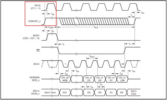
    The datasheet does highlight a timing requirement with respect to CONVST and XCLK. See page 10 of the datasheet, timing specification tS3. The specification describes a required setup time for the rising edge of CONVST to a rising or falling XCLK edge as 6ns. 

    Looks to me like option 1 is the way to go. Officially I'm "The DAC Guy" though, so I'll see if someone from one of the ADC teams will also give this a look in case they have any extra information.

  • Kevin,

    Thank you for the information and for your help. Yes, we saw page 10, but this is listed under Serial connection. The similar timing for the Parallel connection does not even mention this relationship, which is why we thought we would ask and confirm.

    In any event, unless someone comes along and contradicts your observation, we will indeed use the Option 1. We have updated the timing diagram to further clarify the relationship as it pertains to our situation.

    Marc

  • Mark,

    I've asked Tom Hendrick, the engineer responsible for this device, to give this a look as well and give a nod one way or the other. 

  • Hi Mark,

    The sample and hold switches close with the rising edge of CONVST, so that sets the instance of sampling - the conversion starts with the rising XCLK relative to CONVST with the 6ns hold time.  If you are toggling CONVST synchronous to the falling XCLK edge, the conversion will always start with the next rising XCLK assuming you have at least the 6ns setup time, this is true for either serial or parallel operation.

  • Hi Tom,

    Thanks for the information. What you wrote makes sense. However, we'd like to
    confirm one more thing and I appreciate your patience with all of the questions.

    On page 10 of the datasheet, it indicates that there is a 6nS setup time with
    respect to either the rising or falling edge of the external clock, but somehow
    intuitively that does not make sense, and it also does not jive with what you
    wrote above.

    If indeed the setup time is only with respect to the rising edge of the external
    clock, then perhaps in our case it would be best to use the falling edge of the
    clock synchronous with the rise of Conversion Start, which would give us a full
    25nS of setup time.

    Please confirm our understanding...

    Thank you,
    Marc 

  • Hi Marc,

    Sorry for the delay here - I actually went back through the data sheet and realized that the ADS8555 has a slightly different conversion mechanism than what I described last week.  Take a look at page 19, under the CONVST_X description.  The tS3 time is against both the rising and falling SCLK edge because either edge will trigger the start of the actual conversion.  You could sync your CONVSTs with either the rising or falling clock edge and the conversion will start with the next edge.