This thread has been locked.

If you have a related question, please click the "Ask a related question" button in the top right corner. The newly created question will be automatically linked to this question.

TLV5632 does not update the output as expected

Other Parts Discussed in Thread: TLV5632, TLV5604, TLV5614, TLV5630

Hallo,

we're trying to use a "TLV5632" while developping a sensor simulation for automotive concerns. Unfortunately, it does not work as we expected.

The SPI communication to the TLV5632 is done by a STM32F407 microcontroller of STMicroelecontronics.Our hardware configuration of the TLV5632 looks like the following:

-          Mode: not connected (DSP Mode)

-          not PRE: permanent logical 1

-          not LDAC: permanent logical 0

The SPI communication exactly looks like it is specified in the datasheet, when using the DSP Mode. As mentioned, the DAC output should be updated after the 16. falling edge of the clock signal. The same is said in the User's Guide of the "TLV5604/08/31 and TLV5614/10/30 Evaluation Module“, as “When operated in DSP mode, W4 should be closed (MODE = 0). This causes the DAC outputs to update after the 16th falling clock edge”. Unfortunately, we cannot observe that behaviour. Instead, the output is updated after the following rising edge on the FS. What we need is the update of the output immediately after the 16. falling edge of the clock.

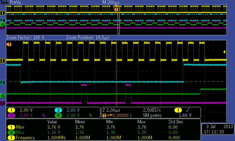
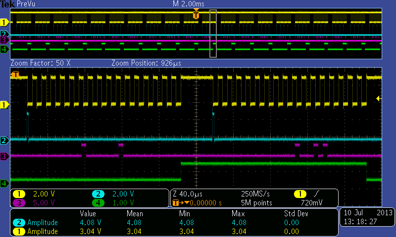
The following screenshots show two spi communications, directly following after each other and the behaviour of the output. That channel mapping is as:

CH1: SCLK

CH2: DIN

CH3: FS

CH4: DAC OUTA

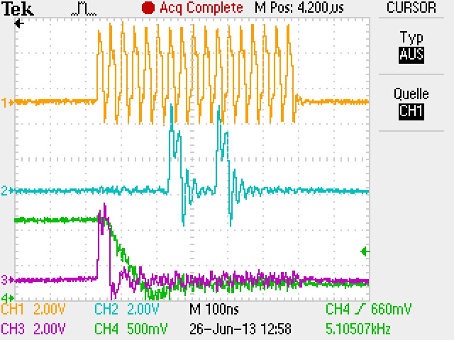
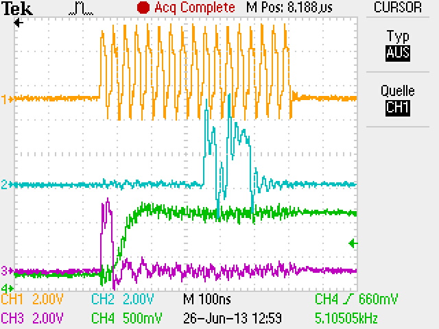
The first screenshot shows the spi command 0x0440, which should immediately update the output voltage to~1,08V. But this can be observed as recently as the next spi command is send (see second screenshot). But at this moment, the command 0x00B0 is transmitted, which should then update the DAC to ~0,17V.

Furthermore, we have the following operation conditions:

- SPI clock @ 30MHz

- Microcontroller is configured to use the "TI mode"

- After startup, the DAC is configured by the commands 0x800E and 0x900F

Do you have any idea, what's wrong and how we could solve the problem?

Thanks for your support!

Chris

  • Hello Christopher,

    Can you try grounding the MODE pin and see if you get any different results? Your SPI looks pretty clean to me - I'll have to get some units in my lab and set this up with a pattern generator to fully test this behavior.

  • Hi Kevin,

    thanks for your reply!

    We tried grounding the MODE pin, but it did not change the behaviour. Looking for a workaround for our problem, we had the idea to disable the SPI interface after each communication step. This results in a high impedance state of the corresponding microcontroller pins. To get a rising edge of the frame select signal afterwards, we used a pullup resistor. This resulted in the expected SPI signals, but neither updated the DAC outputs. Therefore, our assumption that the frame select signal is responsible for the update of the DAC is wrong. Consequently, we supposed that the clock signal is responsible for the update of the DACs ouput. Trying a pullup resistor on the clock signal the same way as on the frame select signal, resulted in the desired update of the output.

    In other words, the output is updated on the next rising edge of the clock signal after the 16th databit has been transmitted. Can you confirm that statement?

    Christopher

  • Christopher,

    That will be precisely what I'm looking for when I take this to the lab. It may take me until Tuesday or Wednesday to get to this though. Thanks for your patience.

  • Christopher,

    Sorry for the delays - I forgot about the holiday coming up in the US last week. We've almost got some information ready for you.

  • No Problem, at the moment our workaround seems to satisfy the requirements. Anyway, we are very interested in your findings.

  • Hi Christopher,

    As you discovered, the update of the DAC output on the TLV5632 is determined by a 17th rising SCLK edge. This is consistent with the datasheet timing diagram, although it’s a bit hard to discern with the uC mode specifications overlapping and multiple don’t care conditions. Desired DAC updating can be achieved either by adding a 17th SCLK pulse, as shown in Figure 1, or by having SCLK idle high, as shown in Figure 2, which you created with your pull-up resistor. I prefer your solution as it retains one SCLK pulse per bit of data and keeps the start and finish of each SPI exchange together instead of the next exchange relying on the 17th SCLK falling edge of the previous exchange.

    In the below oscilloscope captures,

    Trace 1 (yellow) – SCLK
    Trace 2 (blue) – FS
    Trace 3 (purple) – MOSI
    Trace 4 (green) – DACA OUT


    Figure 1 – DACA output updates after 17th rising SCLK edge

    Figure 2 – DACA output updates due to rising edge of SCLK returning to high idle state after 16 pulses


    Jonathan Bender
    Precision DAC Applications

  • Hi Jonathan,

    thank you for your reply and your efforts!

    We will then keep our solution as it exactly results in the communication, that is shown in Figure 2.

    It's true, that the timing diagram shows the 17th rising edge of the SCLK. Nevertheless, there are some other hints indicating that the output is updated after having received the 16th data bit. Precisly I mean the following statements:

    1. After 16 bits have been transferred, the content of the shift register is moved to one of the DAC holding registers, depending on the address bits within the data word. A logic 0 on the LDAC pin is required to transfer the content of the DAC holding register to the DAC latch and to update the DAC outputs. (Datasheet TLV5630/31/32, Page 10)
    2. When operated in DSP mode, W4 should be closed (MODE = 0). This causes the DAC outputs to update after the 16th falling clock edge. (TLV5604/08/31 and TLV5614/10/30 Evaluation Module, Page 24)

    We think, the need of the 17th rising edge should be explicitly pointed out to avoid that other users run into the same problem. What do you think?

    Christopher

  • Christopher,

    The datasheet is a bit misleading regarding when the DAC output is latched. We'll look into modifying the datasheet. Thanks for bringing this to our attention and special thanks for your great patience!