Hello TI E2E community.
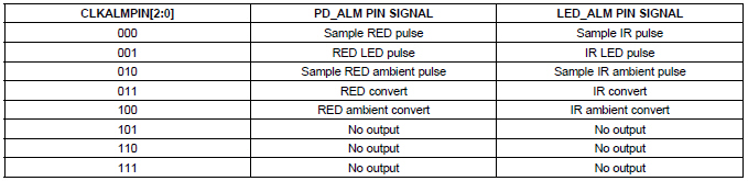
1. I have found a part of datasheet which probably contains an error (or it is not clearly written). It is related to Table 5. on page 60 (SBAS602D - MAY 2013).
1a. What is the difference between "000" and "010" setting? The last column has one word "pulse" in addition but what does it mean?
1b. What is the function of the "100" setting. Does it means - " LED1/2 Ambient SAMPLE clock " or " LED1/2 Ambient CONVERSION clock ".
2. There is a discrepancy in time diagrams on Figure 57. (page 27) and Figure 59. (on page 29). On the first one there are two ADC conversions per one repetition period, but on the second one, there are four ADC conversions per one repetition period. Can you explain more clearly the ADC sampling and conversion procedures.
3. According to the sample averaging mode - it's not clearly written how much averages can be fitted in one ADC cycle. It is related to Equation 3 (page 35). If PRF = 1250Hz we can fit exactly 4 averages/conversions by 50us each. But this means that the last ADC conversion from the current cycle will finish exactly at the moment when next ADC reset pulse appears. Is it possible that the last conversion is invalid in this case and the total averaging of this cycle is incorrect due to this fact? If this is true - probably it's better to use 3 averages in this example (what it's drawn on Figure 66. in fact).
4. In Table 2. (on page 31), all timing cycles are strictly "glued" each to other. For example "End of LED2 pulse" has exactly the same timing like "End of LED 2 sample". I have played a bit with the development kit and I found that the default timings used there are passed with 2 clocks difference. I suppose, this is done to escape from some noises during switching. If this is true - it must be written in the data sheet, also.
5. Is it possible to Read/Write more the one register in single SPISTE low cycle? Page 46/47 do not explain this clearly. For example is it valid to write two registers in the following procedure:
SPISTE->Low, A7-A0, D23-D0, A7-A0, D23-D0, SPISTE->High.
6. Should I set SPI_READ bit before each read cycle? Or write it once is enough if the next operations are only readings? With other words - do i need a write procedure before each reading, or the SPI_READ bit keeps its state until it's changed by the user?
7. As I found in TI E2E discussion related to AFE4490, there are some registers which are write-only (CONTROL0 for example). IIt will be good to specify this in the data sheet for each of AFE4490 registers - is it Read, Read - Write or Write only.
8. And one "application specific" question. All examples on the demo board and in the data sheet, are designed to use relatively "long" LED ON pulses and relatively low Led current. But I thing in some applications it will be better to use shorter LED ON pulses (for example 100us or even 50us) and higher currents (up to 200mA). This will reduce the impact of the ambient light noise. Right?
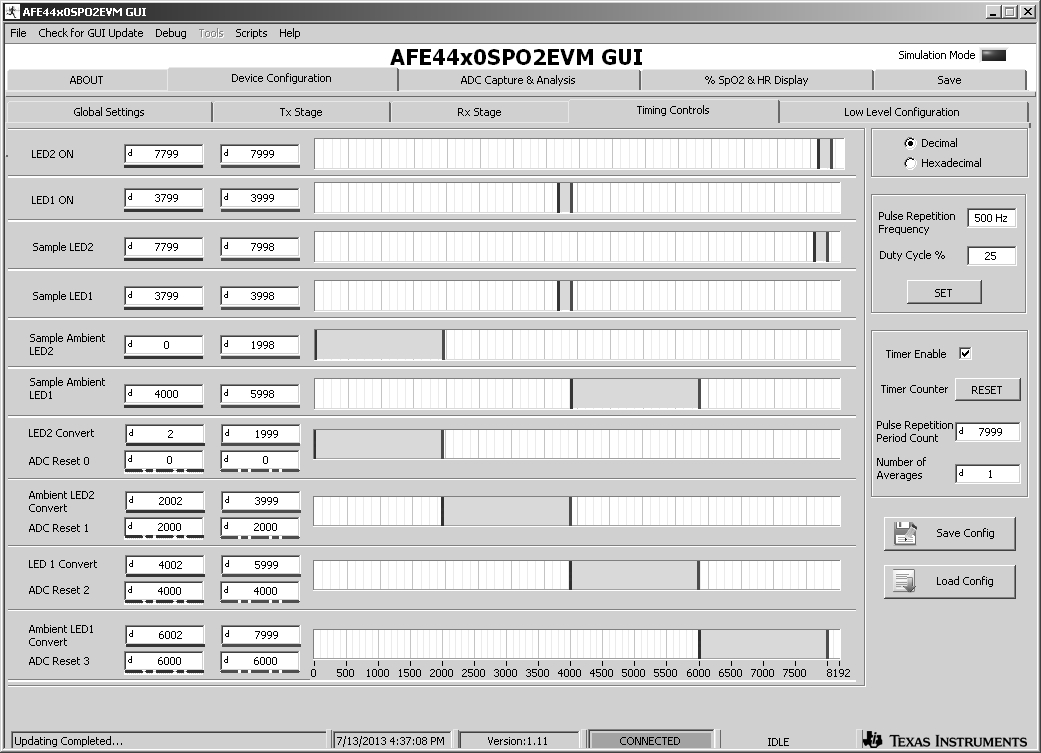
On page 23 is written that the minimum supported sample time is 50uS. Can I use 50uS LED ON and LED SAMPLE times in this case? If this is true, can I use longer conversion times (with a lot of averages), even of lower sampling time? For example can I work with the following timing settings:
PRF = 500Hz (PRT = 2ms), LED1/2 ON time = 50us, LED1/2 sample time = 50us, LED1/2 ambient sample time = 500us, All ADC convertions time = 500us, Averaging = 10.
See next picture:
It's a long list of questions, but this is a chip with complex functions, so normally there is a lot of misunderstandings. Anyway, i think the conception of this chip is really good. And I hope the real result it will cover my expectations too.
Best Regards
Tsvetan Mudrov