This thread has been locked.

If you have a related question, please click the "Ask a related question" button in the top right corner. The newly created question will be automatically linked to this question.

DAC8871 Slew rate

Other Parts Discussed in Thread: DAC8871, DXP, DAC7311, LM7171

Hi.

I am testing DAC8871 EVM with DXP tool. When using the square wave, it looks like the DAC is not meeting the slew rate parameter, mentioned in the data sheet 40V/us.  Maybe I am missing something, could you help?. Attached are the files that describes the measured waveform, DXP configuration and DAC8871 EVM schematic diagram. The signal was measured in J1 connector, pin 2 and pin 6

SlewRate_photos.zip
  • You've already asked this in your existing thread. This discussion will be continued there.

  • Updating this for future readers:

    There are a few things in play here.

    A critical detail of all of this is that the bill of materials shows U2 as an OPA277 while the schematic seems to indicate an OPA211. Double-checking on the EVM I found that U2 is populated with an OPA277. Thanks for bringing this to our attention, I'll need to go back and fix this. As it concerns your issue at hand, though...

    The datasheet specification shows 40V/us slew rate for the unbuffered voltage output, VOUT, of the DAC8871. The measurement made at J1.2 is the output of the OPA277 installed at U2. The OPA277 is an excellent dc operational amplifier, but it's slew rate is only 0.8V/us, so the signal you see at J1.2 is limited.

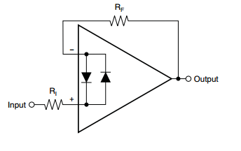
    When you probe J1.6 you're looking at the node that is the OPA277 non-inverting terminal and the Vout pin of theDAC8871. The DAC8871 output at the OPA277 non-inverting terminal is going to attempt to slew at 40V/us but the signal at the inverting terminal is controlled by the OPA277 output and its only going to slew at 0.8V/us. A lot of amplifiers feature back to back diodes to protect the input stage from excessive differential voltages, as illustrated below:

    Since the signal at the non-inverting terminal is moving so much faster than the signal at the inverting terminal, the diodes will eventually forward conduct, shorting the OPA277 output to the DAC8871 input and creating the effect that you've observed. 

    To measure the DAC performance alone you need to disconnect the OPA277 non-inverting input from the DAC8871output. To improve the performance of the whole system you need to replace the OPA277 with a faster amplifier.

  • Thank you Kevin.

    It was removed the OPAM from DAC8871 EVM and the Slew rate was 320ns. Thanks a lot for your support.

    Two more questions about the slew rate. DXP was programmed to generated a square wave at 200KHz. The signal in the oscilloscope is shown in the attached file. The signal get distortioned by the slew rate, in positive and negative voltages.

    I guess that lowering the Vref voltage to 5V, the output voltage will be better, but it was get the same result.

    The questions are:

    * Do I missing something in order to get a clean square wave?

    * If the DAC slew rate can not be reduced, then can you suggest other DAC, in order to get a square wave at 400KHz.

    Regards.

    DAC8871_slew_rate.zip
  • Hello Armando,

    Can you explain the precise circumstances of these captures?

    This was taken at the DAC output with the OPA removed, right? Is there still an op amp driving the DAC reference or is it connected directly to an external reference source?

  • Hi Kevin.

    The capture was taken at the DAC output (Vout), with the OPAM removed, No OPAM is used to drive the DAC output. The waveform was measured at J1, pin 6.

  • There is no amplifier driving the reference input either?

  • The circuit is using the Vref voltages provided by the OPAM U5D and U5C, I mean the switches W3 and W1 are closed at pines 1-2. the ref voltage is +-10V.

  • Armando,

    Thanks for sharing those details.

    In summary:

    • The goal is to create a 400kHz square wave (10 volts peak to peak? Swings from 0-10V?)
    • The screen captures you have delivered are of 200kHz square waves
      • One capture seems to be using a 10 volt reference, swinging 10 volts peak to peak, from 0 to 10 volts
      • The second seems to be using a 5 volt reference, swinging 5 volts peak to peak, from 0 to 5 volts
    • Let me know if I've got any of this wrong now, I'm not familiar with your scope and I'm not sure if I've identified the correct zero crossing
    • The complaint is concerning the "rounded edges" of the square wave

    We created a quick setup here to recreate this. Only difference is we're sweeping from -10V to +10V. You can see similar rounding on the corners:

    What you see in this capture is the DAC output (yellow trace), VREF_H (blue trace), and VREF_L (purple trace). You'll notice the DAC output is attenuated a little bit and some drooping on both sides of the reference. To help this we added a pair of decoupling capacitors to the VREF_H and VREF_L inputs (10uF and 0.1uF) to help the on-board amplifiers source the current necessary to meet this slew rate. Now the output looks quite a bit cleaner:


    Hope this helps.
  • Hi Kevin. Thank you for your answer. I really appreciate you support.

    My goal is to create a waveform generator which can generate square signals at 400KHz, swings from -5V to 5V.

    It was added two tantalum capacitors to VREFH y VREFL signals. I mean It was added one tantalum capacitor to C14 in parallel and other tantalum capacitor to C11 in parallel.Both tantalum capacitors are 10uf, 25V. Is this the action that you recommended?.

    Attached are two oscillocope screens. Both signals use VrefH = 5V, VrefL = -5V. The signal was measured in J1, pin6. The OPAM 277 was removed.

    The questions are:

    * Both signals do not stay at the frequency that was programmed in the DXP, the signal at 200KHz, shows a signal at 166.69KHz and signal programmed at 400KHz, shows a signal at 249.91Khz. Is it needed to add at DAC output an OPAM at its Vout pin, in order to get the right frequency?  

    * Do you have a circuit ready to test, that generates square waves (and all other standard waves) at 400KHz as maximum frequency?.

    Regards.

    DAC8871_screen_vref_pm5V.zip
  • Armando,

    I apologize for my late response.

    Armando Govea said:
    It was added two tantalum capacitors to VREFH y VREFL signals. I mean It was added one tantalum capacitor to C14 in parallel and other tantalum capacitor to C11 in parallel.Both tantalum capacitors are 10uf, 25V. Is this the action that you recommended?.

    The value of the capacitor I used was relatively arbitrary. The idea is just to add some "charge well" to the VREF_H and VREF_L lines to help source current during the very fast slew period of the DAC output.

    Armando Govea said:
    * Both signals do not stay at the frequency that was programmed in the DXP, the signal at 200KHz, shows a signal at 166.69KHz and signal programmed at 400KHz, shows a signal at 249.91Khz. Is it needed to add at DAC output an OPAM at its Vout pin, in order to get the right frequency?  

    This is a digital problem, not an analog problem. If you probe the SPI bus of the EVM you'll see the SCLK is set to 20MHz. Each frame contains 16 bits of data and there's about 200 nanoseconds of time all together between the falling edge of CS and the first SCLK, the final SCLK and the rising edge of CS, and the total time CS spends high (this time doesn't change based on SCLK). We need at least two updates to create a square wave, so we can an equation that describes the frequencies we can achieve based on the frequency of SCLK, fSCLK, and the number of updates per period, n (must be a multiple of 2 to maintain 50% duty cycle):

     So with a 20MHz clock the fastest we can go (purely based on digital I/O, not analog settling time of the DAC), is 500kHz. If we're to keep a 50% duty cycle then we can only increment n in multiples of two to change the square wave frequency. Here's a short table of what that works out to be:

    Possible Output Square Waves w/20MHz SCLK

    n = 2 500 kHz
    n = 4 250 kHz
    n = 6 166.667 kHz
    n = 8 125 kHz
    n = 10 100 kHz
    n = 12 83.333 kHz

    Possible Output Square Waves w/38MHz SCLK

    n = 2 805.08 kHz
    n = 4 402.54 kHz
    n = 6 268.36 kHz
    n = 8 201.27 kHz
    n = 10 161.01 kHz
    n = 12 134.18 kHz

    This is just with the EVM setup. Of course, in your own system, you wouldn't have to provide more than two updates per period of the square wave to realize this square wave. DXP just always provides back to back updates.

    Armando Govea said:
    * Do you have a circuit ready to test, that generates square waves (and all other standard waves) at 400KHz as maximum frequency?.

    I do not have such a reference design on hand at this time. It's something that we can look into sometime in the future, though.

  • Hi Kevin.

    Thank you for the answer.

    I have tried to change the SCLK rate to 38MHz, but DXP tool has not enabled this option. Do you know a way to modify this parameter in DXP tool?.

    DAC8871 supports up 50MHz in SPI port.

    Regards.

  • Armando,

    First, find where the device files are stored on your PC. DXP uses special paths defined on each PC to decide where is appropriate to store it's device files. Go to the root installation directory for the DXP program, on Windows 7 this is usually C:\Program Files (x86)\DXP\. Open the file "dxp.ini", it should look like this:

    [DXP]

    Version =2.0.0

    Build =53

    DXPIndex =C:\Program Files (x86)\DXP\Misc

    DXPDevices =C:\Users\Public\Documents\DXP\Devices

    FWDir =C:\Program Files (x86)\DXP\fw

    SaveDir =C:\Users\Public\Documents\DXP\saved

    MiscDir = C:\work\dxp_v2\misc

    ImagesDir =C:\Program Files (x86)\DXP\images

    ClearCommLog = "TRUE"

    ClearDataDump = "TRUE"

    viSearchPath = C:\Program Files (x86)\DXP\Common Files\*


    [LINKS]

    DXPHome = http://www.ti.com/dxp

    ProductFolderBase = http://www.ti.com/product/

    UserGuideBase = http://www.ti.com/tool/

    PDCForum = http://e2e.ti.com/support/data_converters/precision_data_converters/default.aspx

    The parameter called "DXPDevices", highlighted in yellow above, is what you're interested in. If you go to that location on your PC you can view all of the xml files for the devices installed on your PC. Modify the DACXXXX XML file to change SCLK frequency. Here's an example with the DAC7311:

    <?xml version="1.0"?>

    <device>

      <name>DAC7311</name>

      <revision>1.0.0</revision>

      <date>21Aug2012</date>

      <devicesettings>

        <instructionwidth>16</instructionwidth>

        <channels>1</channels>

        <format>sbinary</format>

        <dataword>CCDDDDDDDDDDDDxx</dataword>

        <commanddefault>0</commanddefault>

        <commandlatch>0</commandlatch>

        <maxupdaterate>1000000</maxupdaterate>

        <interface>

          <type>spi</type>

          <polarity>1</polarity>

          <phase>0</phase>

          <maxsclk>20000000</maxsclk>

          <framebits>16</framebits>

        </interface>

        <latchpin>

          <feature>0</feature>

          <pulsepol>0</pulsepol>

        </latchpin>

        <FSplus>4.096</FSplus>

        <FSminus>0</FSminus>

      </devicesettings>

    </device>

    You want to change the parameter called “<maxsclk>”, highlighted in yellow above, to change the SPI clock for the device. The maximum SCLK for the MMB0 should be 50MHz. You may not get EXACTLY the frequency you type in. The DSP firmware will configure the SCLK to the closest value the clock divider will allow it to get to.

     Hope this helps. Let me know if you have issues.


  • Hi Kevin. Thanks a lot for your support. Very clear your procedure.The frequency change was done without problem.

    One more question, DXP was programmed to generate a sine wave, it was tried several frequencies. The output at DAC8871 EVM, are in the attached files. Is there a procedure where it is explained, how the DXP generates the sine signal and what speed rate is the maximum that we can get using 50MHz SPI clk?.

    The EVM is working with the next parameters:

    Vsupply: +-10V

    Vref: +-5V

    The OPAM U2 was replaced by LM7171, and the signal was measured in OPAM output at J1, Pin2.

    Thanks in advance.

    Armando.

    Sine_wave_SPI_50MHz.zip
  • Hello Armando,

    I'm glad we've been able to deliver good support for your project! Thanks for the positive feedback.

    The MMB0 / DXP are really intended to be "black box" support platforms purely used for simplified evaluation, so we never created any documentation outside of the User's Guide for DXP.

    Basically the MMB0 firmware contains a quarter-wave sine table. This contains data-points for 1/4th of the output sinusoid. The second, third, and fourth regions of the sinusoid are the same data rotated as needed. Based on the frequency of the sinusoid more or less points from the sine table are used to update the DAC output.

    This is a relatively common way to create a sinusoid.

  • Hi Kevin. Thank you for your soon answer.

    When DXP is programmed to generate a sine signal, it sends all the values of DAC resolution?. I mean If it is used a 16 bits DAC, then the DXP sends 65,535 words (1 word=16bit) for a positive cicle and other 65535 words for negative cicle?. This takes to much time, if we consider that each voltage value is 16 bits length.

    I was guessing that DXP only send some significant values, not all. I did some calculation in order to get the maximum sine frequency that can be get, using SPI clock at 50Mhz,,, and according to my calculus, the maximum frequency is 22.439Hz.

    I guess I am missing something, because DXP shows several higher frequency values.

    What do you think?.

    Regards.

  • Armando,

    DXP will only use select values from the sine look up table based on the frequency that it is programmed to generate. The highest frequency sinusoid would end up being a simple two-point waveform.

    The frequency values displayed in the DXP GUI assumes the SPI clock is as it was set in the default version of the XML file at 20MHz. As we've discussed in this thread, some digital constraints exist around exactly what frequency ends up at the output based on the SCLK frequency.