This thread has been locked.

If you have a related question, please click the "Ask a related question" button in the top right corner. The newly created question will be automatically linked to this question.

ADS7828 Read problem

Other Parts Discussed in Thread: ADS7828, TIPD112, ADS7830

Hi.

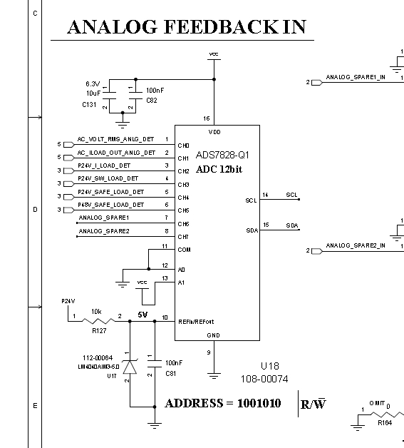
On my last new board design I use ADC TI p/n ADS7828EIPWR. On my debugging I see that I am not get accuracy voltage (ch-0 to ch-7), My connection is single not differential.

I have a 0.1V imprecision on read. means when I enter 2V on CH-0 my read is 2.1V. I also try to enter 0.5V lower input voltage and the result are same 0.1V imprecision but now is down 0.1V (mean -0.1V from real input).

I use external Vref=5V Please advise ?

Note: All my GND and supply voltage lookin good without noise.

Please advise...?

Regards

Arie Gez


  • Hi Arie,

    What are the raw ADC outputs you are reading corresponding to your inputs? You should see some noise in the ADC output when you perform multiple conversions on a DC input. Could you please also share a schematic showing your ADC and drive circuitry (reference, input, supply)?

    Thanks,

    Harsha

  • Hi.

    I put also prob and try to see the I2C signals with oscilloscope and they lookv good without nois also my analog input look good. The data that I see on the oscilloscope this actually what I am read.

    The problem is on the value of ADC conversion,


    Some of of the drive circuits:


    Note: See below measurements with external Vref = 5V

    CH6 - Vin ADC read (Vdc) Diff %
    0.251 0.1927 23.22709
    0.5 0.3779 24.42
    0.801 0.665 16.97878
    1 1.0634 6.34
    1.4 1.547 10.5
    1.6 1.633 2.0625
    1.6187 1.6711 3.237166
    2 2.117 5.85

    As you can see from the table there is a non constant reading offeset.

    Please advise...?


    Thanks

    Arie.


  • Hi Arie,

    The conversion errors you are experiencing are probably due to the input signal not being able to fully settle across the ADC inputs before conversion begins.

    The driver output experiences large high frequency load current transients during the sampling phase, as the ADC's internal sample-and-hold capacitor is switched in and charges to the input voltage. Even if the input voltage has not changed, there is a load transient that occurs due to charge injection from the sampling switch. Anyway, the bottom line is that the ADC input voltage fluctuates during the sampling phase and if it doesn't settle fully before the ADC starts converting, then the conversion result is inaccurate.

    Supplying these high frequency load transients requires a near-ideal voltage source, so we pretty much need to use an external low ESR capacitor at the ADC input to provide most of the required charge. This external "reservoir" capacitor, usually chosen to be >20 x sampling cap value (Csh = 25pF for the ADS7828) is crucial for preventing op amp slew, and it is missing from your driver. A series isolation resistor is also required to decouple the op amp output from the capacitor for stability, and for limiting input noise.

    I would like to recommend the following TI Precision Verified Design as a reference to help you optimize your design:

    http://www.ti.com/tool/tipd112
    http://www.ti.com/lit/pdf/tidu012

    Please have a look and let me know if I can be of any further assistance.

    Best Regards,
    Harsha

  • Hi Harsha,


    Thanks for your prompt replay.

    I have implemented all you suggestions and yet the conversion is wrong.

    Please find attached Excel sheet that show multiply sampling of the same voltage (0.8V and 2V).

    You can see that the reading are quite stable but still with offset.

    Above that the offset isn’t predictable (not linear or…).

    5582.adc read.xlsx


    Please advice,

    Arie

  • Hi Arie,

    I have attached histograms of the equivalent output codes corresponding to your measurements. We should be seeing a continuous gaussian distribution, but as you can see, the output code distribution is non-gaussian and all of the even codes are missing. It looks like you may not be correctly capturing the LSB of the data output or something is wrong in the way you are assembling the serial data bits to generate the decimal output word. What is the formula you are using to convert the serial data output to a voltage reading?

    Missing codes also occur when the reference voltage is not stable during conversion. Can you please probe the ADC reference input and get a scope plot of the Vref signal over multiple conversions?

    Thanks,
    Harsha

    1663.adc read.xlsx

  • Hi Harsha,

     Thanks again for you prompt replay.

    Regarding the I2C bus interpretation we compared the I2C bus as seem on the scope to what we read and it is the same.

    Also at the same board we have other I2C components and its working fine (We have CAT9555).

    The problem that we reported happen the same also with internal 2.5V reference.

    Please find attached scope view of the reference signal during sampling period (2 pictures, one with AC decoupling of the ref voltage and the other with DC decoupling).

    We also measure the ch6 input voltage during sampling period and it the same as the reference (stable)


    Please advice,

    Arie

    AC decoupling

    DC decoupling

  • Arie,

    I need more information to be able to better assist you. Can you please send me a scope plot showing SDA, SCL, Vin and Vref over a complete I2C transaction cycle as the one below:

    This will make it very clear as to what you are feeding the device and the raw data that it is giving out. Even better if you could show me the same plot for multiple inputs (say 2 or 3).

    Now, the Vref plot you have shown is only over a small part of one transaction cycle and this is not enough to get a good idea of how well the reference driver is able to regulate the ref voltage. For this we need to look at how much Vref is dropping over multiple conversion cycles (say 30). So it would be helpful if you could also include a plot of Vref over multiple conversion cycles.

    Thanks,

    Harsha

  • Hi Harsha,

    Please find attached pdf file that contain all your requests.

    Above that we replaced the ADS7828E with ADS7830 (8 bits adc with the same pacage) using the same setup in order to see if the problem related to the PCB, I2C, design,....  We found that it function correctly (see attaced excell file)

    Best regards,

    Arie

    6560.ti response.pdf

    4527.ads7830.xlsx

  • Hi Arie,

    I haven't had a chance to take a detailed look at the data you have sent me. I will do so and send you a response by Wednesday next week. Thank you for your patience.

    Best Regards,

    Harsha

  • Hi Harsha.

    Okay thank you.

    I will wait to your feedback.

    Regards

    Arie.

  • Hi Arie,

    Thank you for your patience. From your scope plots Vref does not show any gross fluctuations during conversion. With the ADS7830 you have validated that you are able to correctly send and receive data over the 400KHz I2C interface. Also, it looks like the linearity of your input drive circuit is sufficient for driving the ADS7830 but not the ADS7828. What does the CH6 drive circuit which provides the "ANALOG_SPARE1" signal look like? Are you observing these gross ADC linearity issues on multiple ADS7828 units?

    At this point it would not be a bad idea to simplify the circuit to minimize the number of variables. I realize that you have tried the internal reference already but please be sure to disconnect the external ref components entirely (except for the 100nF decoupling cap) to avoid loading the internal ref buffer output. Also with regard to the input driver, you can perhaps try using the AD8027 in a unity gain buffer configuration for wideband operation (for quick settling) and use a simple RC lowpass filter for bandlimiting, as shown on pg 21 of the AD8027 datasheet.

    Best Regards,
    Harsha

  • Hi Harsha,

    Regarding insufficient for driving the ADS7828: The plots we sent you show that the input is stable during ADC conversion.

    Above that we already using for CH6 AD8028 in a unit gain.

    Regarding the reference, we tried internal reference with 100nF and external reference omitted. Same problems.

    Since we run out of ideas, is it possible to share our problem with other TI’s expert ?

    Above that we can send you the board we using or just the I2C master + Pc tools (Which is very simple to use) to test it with the Ti’s EVM.

    Best regards,

    Arie

  • H Harsha,

    Regarding "input drive circuit is sufficient for driving the ADS7830 but not the ADS7828", we can't see any problem in the scope plot of the input to CH6, above that we using AD8028 in a unity gain as input stage for CH6.

    Regarding the reference we already tried internal reference with 100nF cap and external reference omitted, same problems.

    Note: We also ordering from TI samples with different product date code and they was be under tests. the results was same, the samles was ADS7828EI, ADS7828EB

    Since we run out of ideas, I would like to ask if is it possible to share our problem with others TI’s expert ?

    Above that we can send you the board we using or just the I2C master +Pc tools (Which is very simple to use) to test it with the Ti’s EVM.

    Best regards,

    Arie

  • Hi Arie,

    Yes, it would be helpful if you could send us your board. Please accept my "friend request" so I can privately send you my shipping address.

    Thanks,

    Harsha

  • Hi Harsha.

    Okay,  Done !

    Waiting to your replay

    Regards

    Arie.