This thread has been locked.

If you have a related question, please click the "Ask a related question" button in the top right corner. The newly created question will be automatically linked to this question.

Question regarding relative phase of multiple ADS5500 digitizer when DLL enabled

Other Parts Discussed in Thread: ADS5500, ADS42JB69, ADS42LB69

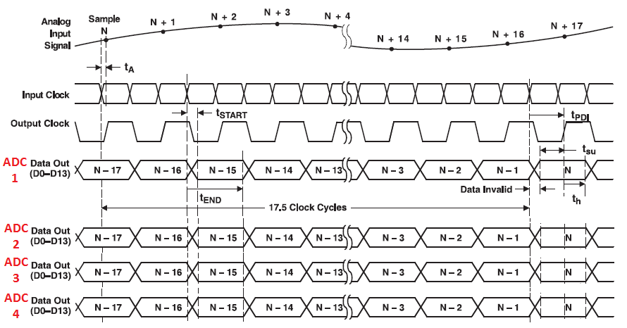
If I have two ADS5500 digitizers with DLL enabled both running off a common clock and measuring the same input signal will the relative phase of the two digital outputs have a fixed relationship from one power up to the next.  There is an attached sketch showing the setup.

ADS5500 phase question graphic.pdf
  • Hello,

    With the ADS5500's internal DLL enabled, the initial clock phase may be different at different start-ups. Therefore, the relative phase of two ADS5500 ADCs may also be different at each start-up. We can confirm with designer to hear their thoughts on possibly syncing the internal DLL so both ADCs can have know relative phase to each other. I believe the possibility is slim since the device was not designed for this. 

    Our newer ADCs such as the ADS42JB69 and ADS42LB69 have dedicated logic input (SYNC or SYSREF) to synchronize the internal clock circuitry. By setting the internal clock circuitry of each individual ADCs to be known, the relative latency of the ADCs can be determined. The ADS42JB69 meets the new JESD204B standard and can meet your deterministic latency requirement.

    -Kang

  • Hi Kang,

    Thank you for your response. We have a follow up question, if we disable DLL will the relative phase of the two digitizers be fixed from one power up to the next?

  • Hello,

    I am waiting for a response from designer. After thinking about this further, I believe that we may still run into the same limitation for DLL disabled. The ADS5500 device has Tstart specifications with typical of 2.2ns and max of 2.9ns. Without the knowledge of the internal chip architecture, we know it is possible that one chip may vary 0.7ns to another when the clock have trigger the capture for both ADCs. Since there is no minimum of the spec, we cannot predict the range of variation. Therefore, I believe that we may still not able to reliably estimate the latency difference between the two ADCs when they have a shared clock.

    -Kang

  • Hi,

    We plan to calibrate out the fixed delays and timing offsets between two A/Ds. Our question is: Will the delays and offsets vary by more than 10pS from one power up the the next, or over time?

  • Hi,

    Sorry for such a long delay on this issue. To make sure we're on the same page about what you're trying to do, let me lay out how I would go about synchronizing multiple parts. I think the key here is using the input clock to the ADCs to capture the data in the FPGA rather than the output clock. See the block diagram below. The key timing specs are the total latency of the ADC (fixed at 17.5 clock cycles) and the tSTART and tEND parameters that define the data valid window relative to the input clock. If you match all of the clock trace lengths to the ADCs and FPGA and the data trace lengths from the ADCs to the FPGA, then this all simply comes down to meeting the timing constraints for all data bits (from all converters) relative to the single input clock to the FPGA based on the tSTART and tEND parameters in the datasheet. It should be no more difficult than achieving timing for a single ADC using the input clock to capture the data instead of the output clock, except for trying to meet timing with N times more data bits. In fact, the data trace lengths could be different if you account for the differences in your timing constraints as well.

    Using the method above, the total data valid window is only 2.9 ns (tEnd(min) - tStart(max)). I'm guessing that we're on the same page as far as the method and that this small window is the reason for the inquiry. Unfortunately, our timing constraints are the worst case scenario across voltage and temperature and from part to part. This is usually sufficient for high volume production because individual delays cannot be calibrated out in mass production. For that reason, we do not usually characterize the worst case timing variance for a single part. 

    So, I think the simple answer to your question is that we cannot guarantee that the offsets won't vary by more than 10 ps for a single part. The best we can guarantee is the tpd spec that's listed in the datasheet. I wouldn't expect a single part to vary over the full range of the tpd spec, but I would guess that the part will vary more than 10ps over temperature alone. However, for fixed operation conditions (voltage and temperature), a single part should exhibit little variance from startup to startup, but we do not have this characterized. The best we can do is measure a single part on the EVM from startup to startup to see the variance.

    Regards,
    Matt Guibord