This thread has been locked.

If you have a related question, please click the "Ask a related question" button in the top right corner. The newly created question will be automatically linked to this question.

Reg MSC1210y5 program is frequently deleted.

Other Parts Discussed in Thread: MSC1210Y5, MSC1210, LM1117, MAX232, INA826, TPS3837


Hello sir,

                I am using MSC1210Y5 controller for weighing scales. I have supply new product our client. product is operation is working fine. but frequently program was deleted. after reprogram this product its working fine. again within 2 month program was automatically deleted.

        I am used code memory (Decimal 30510 byte, Hex 0x7724),data memory is (Decimal 750 byte, Hex 0x2EE),Memory is configured program memory is 30k and data memory is 2k.

I am used LIPO battery 12v 4800 mAH, and peripheral is lcd, GSM modem load cell and one more face reader, can you give solution for frequently code memory is erased. I am waiting for your reply.

Thanks and regards,

Ramesh k

  • Hi Ramesh,

    When you say erased, do you mean that all bits show 0xFF for each byte in memory?  Does this happen just with program memory or does data memory change as well?

    If only a portion (random bytes) are affected, this is usually due to a transient event.  If there are pages of memory erased, this is usually due to a random programming condition that accidently erases a page in program memory instead of the data memory allocation. 

    I'm guessing this is transient related.  Even though your system is battery operated, other sources of noise can enter your system externally from motors, transformers, and othe EMI sources.  Can you tell me something about the environmental conditions this system is in?

    Best regards,

    Bob B

  • Dear Bob,

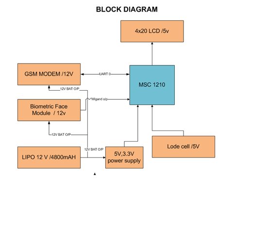
                  This post last day only i am posted, sorry, i am not post before. thanks for your valuable reply.i have placed my block diagram bellow, kindly find and update your solution. I am facing problem  for msc1210. my product is working fine, suddenly program wash in our micro controller after reprogram controller is working fine, while erased program my LCD nothing to show data, and check UART0 this Data also cant communicate.so kindly update any other test procedure. kindly update solution.

    Thanks and regards,

    Ramesh k

  • Hi Ramesh,

    Thanks for sending the block diagram.  Unfortunately this doesn't tell me too much other than the system is probably in a remote location.  We still need to know what memory is erased (or corrupted), or how much memory is being affected.

    If you are able to reprogram the MSC1210, you should be able to read the contents out to a file and compare what is currently stored in program memory to the correct data.  This would be the first place to start.  We need to know what areas are being affected.

    Best regards,

    Bob B

  • Dear Bob,

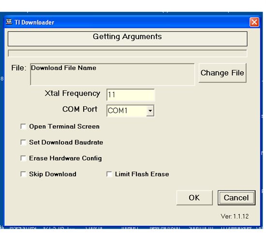
                         Thanks for your valuable reply, I am using ti down loader, I think its not read option, I have given bellow screen short ti down loader, can you guide me how can i read the data from MSC1210 using Ti down loader .

    now i did reprogram MSC 1210, so I will be wait next time corrupt MSC1210. it will take may be one month. then only i will get read data from msc121o.

      To my knowledge our program memory is corrupted. because display cant show data. if data memory is loss, Lcd will be display any data string message, I am not sure can you conform?. Thanks,kindly  i am wait for your reply.

    Thanks and regard,

    Ramesh k


  • Hi Ramesh,

    If you click on "Open Terminal Screen" and "Skip Download" you will open a console terminal window where you can read out the contents of the memory.  Commands are given in the following document in Table 1:

    ftp://ftp.ti.com/pub/data_acquisition/MSC_CD-ROM/Application_Notes/sbaa076b_Programming_the_MSC1210.PDF

    Best regards,

    Bob B

  • Dear Bob,

                         Thanks for your reply, I will try read from MSC1210, I got terminal from ti down loader, i am connect working hardware try to read , and give  read command XRnnnn  but i got junk 15 byte only can you brief note or doc for read it. I am waiting for your reply.

    Thanks,

    Ramesh k


  • Hi Ramesh,

    To read the program memory the command is CRnnnn.  The nnnn refers to the address location. For example, CR0000 should return the first 16 bytes of code memory.  This assumes that the security bit in the HCR0 configuration registers has not been changed to '0'.

    Best regards,

    Bob B

  • Dear Bob,

              Last week two device was corrupted program. I have attached xlsx sheet bellow link.

    4555.MSC1210_Program_Problem_Report.xlsx

    1) Device ID 3 is ADC Weight only cant updated in display. i think that part only failed.

    2) Device ID 1 is all program was corrupted. after reprogram works fine.

    3) I have read both device after fail program. that command following bellow.

         XN0000 and CR0000.

    4) Both result i have attached the above link, Kindly update me.

    I am waiting for your reply.

    Thanks and regards,

    Ramesh k

  • Hi Ramesh,

    From the data it looks as if the flash is changing by one bit in the byte value.  We only are seeing a small portion (16 bytes) of data that is probably hundreds or thousands of bytes in total.  There is a couple of things that would still be helpful to know. 

    • What is DVDD for the MSC1210?
    • What crystal frequency is being used?
    • Are you changing from the default values of the FTCON, MSECL and MSECH registers?

    When the erase to the memory takes place, there must be sufficient time to charge the memory cells high so that each byte becomes 0xFF.  So erasing sets the bits.  You cannot write a '1' to a bit, you can only write '0'.  It may be that not enough erase time is being issued to set the bits to the necessary charge.  Or it could be a transient event that is clearing a bit.  The answers to the above questions will help me to determine if there is enough erase time for maximum endurance.

    Best regards,

    Bob B

  • Dear Bob,

                           Thanks your reply. i have given bellow details    

    • What is DVDD for the MSC1210?                 =>3.3V   LM1117- 3.3v
    • What is AVDD for the MSC1210?                  =>5V        LM1117 -5V
    • What crystal frequency is being used?       =>11.0592 oscillator
    • Are you changing from the default values of the FTCON, MSECL and MSECH registers?

         Note:                  

    • FTCON, MSECL and MSECH        => This register i am not used in this code.but its have in reg1210.h file only. that sfr default value is given bellow.

       Reg1210.h

      sfr FTCON  = 0xEF;

      sfr MSECL  = 0xFC;

      sfr MSECH  = 0xFD;

    If you need any detail or schematic, i will send you , kindly update me.

    Thanks and regards,

    Ramesh k

  • Hi Ramesh,

    There are a couple of things that greatly effect the flash endurance.  One is the voltage used when erasing and writing, and second is the time required to effectively erase or write the flash.  The default values in the SFR are based on a 1MHz crystal.  Using a faster crystal reduces the times for erase and write.  I'm not sure if the TI Downloader program adjusts SFR registers for the correct timing.

    The values shown in the reg1210.h file are the addresses associated with the register names.  Using the default values for the registers at the crystal frequency you are using is on the edge and may not adequately erase/write to the MSC1210.  If you have another device that fails, before programming check the following register contents with the console terminal commands:

    RREF (reads the status register FTCON)

    RRFB (read the status register USEC)

    RRFC (reads the status register MSECL)

    RRFD (reads the status register MSECH)

    It would be helpful to know the above values.  I would suggest that the following values be written to the SFR prior to erasing or programming:

    RWFB0D (sets USEC register so write time is about 38us)

    RWFC5D (sets MSECL register)

    RWFDC4 (sets MSECH register)

    The above values will allow for longer erase and write cycle time.  Mass erase of programming memory can be done with:

    M0000

    Best regards,

    Bob B

  • Dear Bob,

                           I will do your point, i have one doubt, I am using oscillator in MSC1210 , I am using 5v power supply to oscillator(OCX-7050 -11.0592 Mhz). can you conform it will affect program corruption.

    Thanks,

    Ramesh k

  • Hi Ramesh,

    The oscillator output should match the DVDD voltage if possible.  There is an internal diode clamp to DVDD.  This will either clamp the output of the oscillator to a lower voltage, or may acutally affect DVDD to a higher output.  The oscillator output should really match DVDD.  It is difficult to say if this mismatch will have an effect on the operation of the MSC1210 or the flash.

    Best regards,

    Bob B

  • Dear Bob,

                          Thanks for your valuable reply. Now i have changed DVDD 3.3V to 5V and Oscillator is AVDD 5V to DVDD 5V , now i have apply  oscillator power is DVDD 5V. is it fine?, Then i  used HCR1= db 11111111b, but i am not use one more register   LVDCON , is it mandatory? so both power supply is AVDD 5V and DVDD 5V so what can i set this register. both register will be affect flash memory? kindly conform me.

    Thanks andregards,

    Ramesh k

  • Hi Ramesh,

    I do not see the pictures that you attached.  The HCR1 settings you selected turn off the brownout detection.  The default LVDCON settings for AVDD and DVDD voltage detection is 2.7V.  You do not need to change these settiings unless you wish to set the detection threshold higher.

    My question to you is are all digital devices communicating with the MSC1210 now running at 5V?  If not, you need to be very careful about mixing voltage levels within your system. 

    Best regards,

    Bob B

  • Dear Bob,

                        Thanks for your reply, I changed power supply DVDD 3.3V to DVDD 5V, and Oscillator power supply before i am given AVDD 5V, now i changed oscillator power supply is DVDD 5V. is it fine?,  i need one more clarification i am using HCR1 register values = 11111111b, now i changed power supply for DVDD 5V , so HCR 1 register need any change?, is it affect FLASH memory and code?. what can i set HCR1 register. and  i am not use one more register LVDCON register. is it mandatory? now i am used AVDD=5V and DVDD=5V. HCR1 is DVDD default is set 2.5V. now i am apply 5V power supply but  i am not change HCR1. can you clarify for me?

    Thanks and regards,

    Ramesh k

  • Dear Bob,

                         My question to you is are all digital devices communicating with the MSC1210 now running at 5V?  If not, you need to be very careful about mixing voltage levels within your system.

           I am not get the above point. can you briefly update me? MSC1210  i changed DVDD 5V, which one best DVDD 3.3v or DVDD 5V.  i used  AVDD 5V and DVDD 5V both separate regulator power supply.

    GSM modem using 12V power supply but read uart TTL 5V using Max232 ic. is it affect MSC1210?

    Thanks,

    Ramesh k

  • Hi Ramesh,

    The values in the HCR1 register sets the point where a device RESET will occur if the function is enabled.  The values you have selected has this function disabled.

    The LVDCON register is very similar except instead of generating a RESET it will trigger an interrupt, assuming this interrupt is enabled. So unless you have this function enabled, nothing will happen. If you do enable the interrupt, you will need to write a handler routine.

    If you want to use either of these functions (brownout detect or low voltage detect), then you will have to enable them.  I can't tell you what to set the levels at as this will relate to your system and the supply operation.  You will need to decide if you want the MSC1210 to issue a RESET if the voltage drops below a particular voltage.

    Best regards,

    Bob B

  • Hi Ramesh,

    A mixed voltage system does not usually work well together.  Most CMOS devices have ESD protection cells that act like a diode connection to the supply.  A 5V device output will force current through the ESD cell to the supply if the supply is 3.3V.  This can damage the device.  This is what you had with the 5V oscillator.  If the MAX232 is also running at 5V, then this could also have damaged the MSC1210 running at 3.3V.

    The absolute maximum table in the datasheet specifies that a digital input cannot exceed DVDD+0.3V relative to DGND.  This means that any input over 3.6V will exceed the absolute maximum ratings for the MSC1210.

    If all devices connected to the MSC1210 are operating at 5V, why was the DVDD of the MSC1210 operating at 3.3V? 

    Best regards,

    Bob B

  • Dear Bob,

                 Thanks for the reply. 

    I have understood your clarification from the last conversation.

    I could not understand  below points please explain me.

    The absolute maximum table in the datasheet specifies that a digital input cannot exceed DVDD+0.3V relative to DGND.  This means that any input over 3.6V will exceed the absolute maximum ratings for the MSC1210.


    If all devices connected to the MSC1210 are operating at 5V, why was the DVDD of the MSC1210 operating at 3.3V?


    From your previous conversation you explained like MSC1210 DVDD voltage should not exceed at  3.6V(above yellow color highlighted).

    Currently I have modified  hardware design of  MSC1210 DVDD and AVDD  voltage as 5V , this means DVDD(5)+0.3V = 5.3V ,will it work fine?.

    Please clarify this .

    Please let me know MSC1210 DVDD  exact operating voltage.

    Thanks and regards,

    Ramesh.K


  • Hi Ramesh,

    All information is in the datasheet.  DVDD can range anywhere between 2.7V and 5.25V in normal operation.  What I was trying to explain before is you should not mix different logic levels and voltages in your system.  When the MSC1210 is operating at 3.3V, it doesn't like to be driven by components operating at 5V.  As long as all the digital components connected to the MSC1210 is running at the same voltage you should be ok.  So operation at 5V is fine.

    Best regards,

    Bob B

  • Dear Bob,

                        Thanks your reply. I will check in field, i f i will get any problem, i will update to you.

    I am satisfy your valuable reply.

    Thanks and regards,

    Ramesh k
  • Dear Bob,

                       As per our previse mail discussion for MSC1210Y5 code corruption. Now testing in site condition

    My program part of code something corrupted, particular module function corrupted. but program not completely corrupted.

    Problems bellow,

    1)Many time weight can't display in lcd , other functions are works,

    2) cant read keypad, some time

    after reprogram everything works fine few days then part of function corrupted.

    Kindly give any solution for me.

    Thanks and regards,

    Ramesh k

  • Hi Ramesh,

    Thank you for the update.  We suspect that transient events can effect the FLASH.  Is it possible that a transient event has occured such as ESD, power transient or surge?

    Best regards,
    Bob B

  • Dear Bob,

                        I have observe a point, That is power on device that day working fine after switch off. then next day switch on device working but part of function corrupted. so many time this kind of problem is accrued.kindly give solution for me.

    one more request kindly send how can i read or download complete hex file data from Flash memory. you will send that command because i will download complete hex code and compare with original hex file.

    Thanks,

    Ramesh k


  • Hi Ramesh,

    Unfortunately we do not have a specific program that I'm aware of that will read the entire FLASH contents and store to a file. There is no specific command to dump the entire memory contents within the device ROM.

    It is very difficult to say what is going on with your board.  I suspect that some transient is affecting the FLASH.  This transient could even take place when turning on the power.  You need to make sure that there is low inductance within your ground path back to the supply.  You also need to make sure that none of the Absolute Maximum Specifications are being violated.  You should have protection from transients on the power supplies (TVS diodes for example) as well as any analog/digital inputs of the MSC1210.

    Best regards,

    Bob B

  • Dear Bob,

                     Thanks your reply, I was read one more TI forum that is MSP430F6x11 This controller also same problem flash memory corrupted,  that guy posted, so many people facing this problem, Kindly check that forum also both are same problem facing. but that forum solution they got?, May be that is also helpful for us.

    Note :

              The same problem MSC1210 I saw one more Ti forum , you also given some solution that link bellow, Kindly check it and what you suggest to him, Ti controller flash corruption facing everybody.

    http://e2e.ti.com/support/data_converters/precision_data_converters/f/73/p/224384/790453.aspx#790453 

    Thanks and regards,

    Ramesh k

  • Hi Ramesh,

    First of all let me say that you cannot necessarily connect issues with the MSP430 and the MSC1210.  They are two entirely different products and the architecture is much different.  Also let me clarify that when you use the word 'many people' are having this issue that there are hundreds if not thousands that do not have a problem as compared to the handful that are having issues.

    That is the differences, so let's look at commonality. For the MSC1210 thread that you referenced, the issue was related to a transient event.  I have already shared this same information with you in this thread as well.  You need to adequately prevent transients from getting into the supply pins or input pins of the MSC1210.  There are many different ways to do this including TVS diodes and ferrites, although ferrites can cause issues on the supply inputs.

    Most recently you have discussed the Flash corruption may be taking place relative to power on/off.  How might this happen?  In the case of the MSP430, the problem appears to be an issue not so much on power up, but on power down where the device is still powered at a lower voltage.  It is suspected that the Flash controller may be unlocking the Flash or there may be an inadvertant jump to Boot ROM code or code space that might accidently call the Boot ROM routines.  At some point while the MSC1210 is powering down there may be a point where the actions of the device are in an unknown state. This would have the same behaviour as a brown out.  We have also discussed this within this thread as well as the configuration within the HCR1 register.  You were using the default values where the brown out detect is disabled.  It is also possible to have a brown out like condition on power up.  If the voltage takes a dip through the power on reset voltage, there may also be an issue where the MSC1210 may operate in an unkown state.  This is some of the problems that the MSP430 customers were also seeing.

    You should set the values of the HCR1 register to the appropriate values so that when the voltage begins to fall the MSC1210 will be held in reset.  This will prevent the device from doing any unwanted action.  Another possibility is to place a supervisor on the Reset pin to hold the device in reset until a specific amount of time has passed following either power up or brown out conditions.  I would suggest that at the very least you properly set the HCR1 values, but it would be even better to use a supply supervisor driven by DVDD supply and connected to the Reset pin.

    Again I want to emphasize that all of your digital circuitry should be running at the same voltage.  You should not be mixing voltages within your system.  Connections between analog and digital ground should also be a low inductance connection (no narrow traces between them.)  If you send me your schematic and layout I can look for any other possible issues.

    Software can also cause problems if interrupt vectors are undefined or if code can inadvertantly jump to invalid code space.  Here are some good coding tips, however some of the information does not apply as the devices are different.  Look for the more generic principles like filling empty code space:

    http://processors.wiki.ti.com/index.php/MSP430_Flash_Best_Practices

    Best regards,
    Bob B

  • Dear bob,

                   Kindly don't mistake me the above word, i saw the forum and sent link to your reference. don't mistake me, as per your above mail you asked schematic so i have attached PDF this link  find it and give solution. last post you update born out detect need to set ib HRC1 register. so i will do set this register and test this status also. kindly review my schematics and updated me. now i changed DVDD3.3V to DVDD_5V now digital supply working DVDD_5V only.

    I have attached schematics for power supply and controller board PDF please kindly update me.

    8814.ecd-106-schematic updated.pdf6266.ecd-107-schematic updated.pdf

    Thanks,

    Ramesh k

  • Dear bob,

                   Kindly don't mistake me the above word, i saw the forum and sent link to your reference. don't mistake me, as per your above mail you asked schematic so i have attached PDF this link  find it and give solution. last post you update born out detect need to set ib HRC1 register. so i will do set this register and test this status also. kindly review my schematics and updated me. now i changed DVDD3.3V to DVDD_5V now digital supply working DVDD_5V only.

    I have attached schematics for power supply and controller board PDF please kindly update me.

    6320.ecd-106-schematic updated.pdf

    8311.ecd-107-schematic updated.pdf

    Thanks,

    Ramesh k

  • Hi Ramesh,

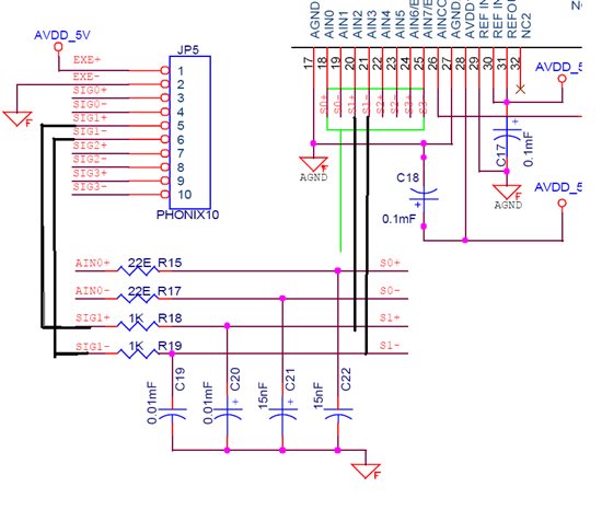
    What I cannot see from the schematic you sent is the analog inputs and how they are connected.  You must make sure that no inputs can exceed the Abosolute Maximum Ratings of the MSC1210.  For example, there is U6 which shows power coming from the 12V supply.  I cannot tell if this device gets connected to the MSC1210, but if it does, you must make certain that the output of the INA does not inadvertantly float to some value above 5V or below AGND.  This may require additional components to ensure this.

    This requirement is also true for any digital signal that may be wired to the board.  Also make sure that power supply transients from turn on or turn off do not cause an Absolute Maximum Specification to be violated.

    Best regards,

    Bob B

  • Dear Bob,

                      I have attached newly updated schematics, kindly find the bellow link for updated PDF.

    i cant use U6 its use for feature its using 12v for EXE+ and GND for EXE-, ADC input is using differential input. you will see schematic.

    4075.ecd-106-schematic _3_updated.pdf

    6646.ecd-107-schematic updated.pdf

    Thanks,

    Ramesh k

  • Hi Ramesh,

    Thanks for the additional information.  Something I didn't notice when giving my previous response is you have AVDD connected to REFIN+ and REFOUT.  If you are using 5V as your reference, then you should not connect the REFOUT pin to the REFIN+.  Having both references connected will cause an issue as the default register settings on power up is to turn on the internal reference.  Even if your program turns off the reference, it will still be competing with the 5V supply until the register is reconfigured.  This means you either need to disconnect the AVDD supply from REFIN+ or you need to disconnect the REFOUT from REFIN+.  You should not have them both connected at the same time.

    I'm confused by what you were trying to tell me about U6.  Is the INA826 (U6) actually connected on your board?  This is not properly connected on the schematic, and even if it were connected properly it can cause serious problems.  The Absolute Maximim input to any of the analog inputs is AVDD+0.3V and AVSS-0.3V.   U6 would potentially be in violation.  Your other analog inputs may be in violation as well.  As I do not know where the SIG signals originate, they must be referenced to AVSS where the inputs remain within the correct common mode of the MSC1210.  Your inputs, both analog and digital, must be protected so as to not allow an out of Absolute Maximum condition.

    Best regards,

    Bob B

  • Dear Bob,

                       Thanks for your reply, i have used AVDD connected to REFIN+ and REFOUT  our design, Its have followed by TI reference design(EVM) there AVDD connected to REFIN+ and REFOUT. I am using Internal reference for 2.5V. Now i am using AVDD_5V for load cell power supply( EXE+, EXE_ ). i am using 5v operating load cell, its connected to RC filter only. its differential inputs.

    Note: If i want use 12V operating Load cell(sensor input), when i will use INA U6 connected channel. IT is operating 12V.

            you have asked , Is the INA826 (U6) actually connected on your board?, yes its connected one Channel remaining channel directly connected differential input using RC Filter.  image given bellow. its connected via net.


    Thanks,

    Ramesh k


  • Dear Bob,

                       Thanks for your reply, i have used AVDD connected to REFIN+ and REFOUT  our design, It’s have followed by TI reference design(EVM) there AVDD connected to REFIN+ and REFOUT. I am using internal reference for 2.5V. Now i am using AVDD_5V for load cell power supply( EXE+, EXE_ ). i am using 5v operating load cell, its connected to RC filter only. its differential inputs.

    Note: If i want use 12V operating Load cell(sensor input), when i will use INA U6 connected channel. IT is operating 12V.

            you have asked , Is the INA826 (U6) actually connected on your board?, yes its connected one Channel remaining channel directly connected differential input using RC Filter.  Image given bellow. It’s connected via net.


    Thanks,

    Ramesh k

  • Hi Ramesh,

    I'm not sure which schematic you are referring to, but the MSC1210EVM schematic that I drew did not have AVDD, REFOUT and REFIN+ connected together.  You should not connect the 5V supply and the 2.5V reference output together.  If you are using the reference at 2.5V, you should disconnect AVDD from the REFOUT and REFIN+ pins.

    The INA826 has the REF pin floating.  This means that there is no common mode established for the part.  This also means that the output of the INA could float anywhere with the range of the supply.  This also means that the Absolute Maximum Ratings can be violated if the output floats above AVDD.  You should either tie the REF pin of the INA to either GND or at mid-AVDD supply to set the common mode of the INA.  You must also add protection so that it is not possible for Absolute Maximums to be exceeeded.  One way to add protection is to change the value of the resistors R15 and R17 to at least 1.4k ohms.

    I would also suggest that you change the RC that is on the RESET pin of the MSC1210 to a supply supervisor.  This will ensure that the MSC1210 is held in RESET for a sufficient amount of time on power up and will also hold the device in RESET if a brownout should occur.

    Best regards,

    Bob B

  • Dear Bob,

           Thanks your reply, i am not get your point meaning I would also suggest that you change the RC that is on the RESET pin of the MSC1210 to a supply supervisor.  This will ensure that the MSC1210 is held in RESET for a sufficient amount of time on power up and will also hold the device in RESET if a brownout should occur.

    I have used reference for below linked document for ADC reference, J8 connection kindly refer this below link

    2100.MSC1210EVM_UG.pdf

    Kindly update adc reference using schmatic,

    Note: I have notesed one point for program fail, i have download hex file using lower baudrate(2400) some board its not curroupted program (upto 2month), but some device downloaded high baudrate(38400) that board weekly ones or two weeks ones program currupted,   kindly give your solution for me.

    Thanks,

    Ramesh k


  • Hi Ramesh,

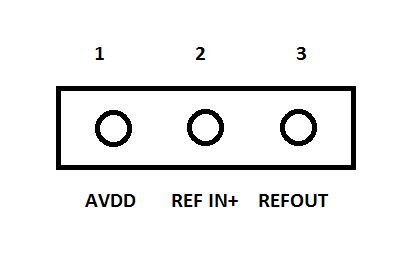
    You are asking about three different things, so I will answer slightly out of order.  Let's discuss the reference first. The J8 jumper for the EVM is default connected to the internal reference of the MSC1210 (page 18 of the user's guide you attached.)  Yes, you can connect to the external reference voltage directly to the REFIN+ and REFIN- pins, but to do so you would have to disconnect the jumpers and connected directly to the two center pins of the jumper.  By removing the jumpers you disconnect the internal reference.  You should not, must not connect an external reference and the internal reference together at the same time.  The sole purpose of the J8 jumper is to prevent this condition.  If you want to use a jumper to be able to choose either the internal reference or the AVDD supply as the reference, then you must use a different jumper configuration.  You can leave REFIN- connected to AGND, but the REFIN+ jumper must be something like the following:

    In this configuration you can connect pins 1 and 2 (AVDD as the reference) or pins 2 and 3 (MSC1210 internal reference).

    For the reset pin on the MSC1210 you have an RC combination.  There duration of time the MSC1210 is held in RESET will depend on the RC time constant relative to the logic voltage required to bring the device out of the reset condition.  This only has value when power is applied.  If a brown out condition should take place, the RC reset circuit will not force the RESET pin high.  A supervisor like the TPS3837 will do this and hold the MSC1210 in RESET for a predetermined amount of time both on power up and for a brown out condition.  This is not a requirement, but may help with the FLASH issue.

    As to the baud rate on the device write, this should really not be an issue.  The flash write time will be based on the master clock frequency (determined by the oscillator connected to the MSC1210) and the configuration of the SFR registers FTCON, USEC and MSEC (which is a combination of MSECH and MSECL).  The correct value for these SFRs should be set by the TI Downloader program based on the XTAL frequency given in the dialog box.  The flash page erase time should be between 4ms and 10ms, and the flash write time should be 30-40us.

    Best regards,

    Bob B


  • Dear Bob,

                          Thanks for your valuable reply. I got very clarity for ADC reference i understood my mistake,i will correct it.

    can you conform you have mention this point (You can leave REFIN- connected to AGND,) so can i do open connection for  REFIN-, (NC) is it ok,

     if we change adc REF properly ,  is it possible for to avoid  flash memory memory corruption,

    Thanks and regards,

    Ramesh k

  • Hi Ramesh,

    REFIN- must have a connection.  If the reference used is the internal reference, this connection is AGND.  If the reference used is AVDD, then the connection for REFIN- is also AGND.  In both cases the reference input for REFIN- is AGND.

    We do not have any certainty as to the cause of the FLASH corruption issue.  We do know that the reference connection you are using is incorrect and can cause damage to the MSC1210.  Can this improper connection cause issues with the FLASH?  Possibly, but we cannot be certain that this is the cause or the only cause.

    Best regards,

    Bob B