This thread has been locked.

If you have a related question, please click the "Ask a related question" button in the top right corner. The newly created question will be automatically linked to this question.

ADS62P42 CMOS MUX mode only deliver B input...receive garbage for input A

Other Parts Discussed in Thread: ADS62P42, DAC5672

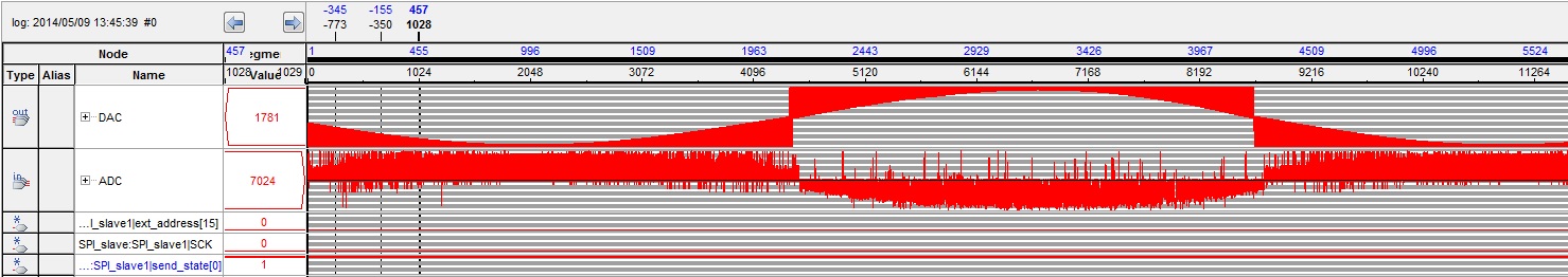
As described in the subject I'm using the ADS62P42 in CMOS MUX Mode and I'm receiving the result for Input B and I'm getting garbage near noise for input A. If I switch I and Q I can really see that the problem is comming from input A. Is there some SPI register values that can be miss-set like a different gain for input A ? I have to mention that all 3 parallel control pins are at GND to have serial (SPI) config only and that I put in register 14 the power down mode at 111 (MUX mode)
Here are the content of my spi registers

register 00 0x02 //at the beginning to reset everything

register 10 0x00
register 11 0x0c
register 12 0x00
register 13 0x10
register 14 0x80
register 16 0x00
register 17 0x0c
register 18 0x00
register 19 0x00
register 1A 0x80
register 1B 0x03
register 1D 0x00

  • Hi Mathieu,

    You should just need to set register 14 to 0x83. I'm assuming you've done this per your description, even though the register's you copied here don't match.

    Make sure you are in SPI mode. RESET should be held low.

    If there is still garbage on Ch A, this might point to a timing error in the FPGA.

    Regards,
    Matt Guibord

  • I have made a mistake while pasting...I have put 0x87 in register 14 not 0x83 like you wrote in your reply. I'm pretty sure the timing is OK since I have sampled twice the frequency to see if I was missing a value and the result was I had the same pattern but with more values.

    I should add that I know that I<m in SPI mode since I can switch from reset and mux mode with my program and I can see the  out put change with Signaltap (Alterra)

  • Hi Matthieu,

    Oops, 0x87 is the correct value, not 0x83. I don't understand your comment about the timing. How did you verify the timing was okay?

    Screenshots of the caputre output would be helpful.

    Regards,
    Matt Guibord

  • The ADC is clocked at 34 MHz (posedge input A negedge input B can be reverse) so at every posedge of 68 MHz there is a value....I have took 136 MHz for the logic analyzer of Altera called signaltap and didn't see a difference in the pattern. I have a square wave on input B and a sine wave on input A and only seeing a filled square wave at the output of the ADC (so I have a square wave for B input and noise for input A so it fill the square wave. You can look at the picture below to see that I have my transmitter chain (DAC+modulator+...) DAC line is the input of the DAC5672 and ADC is what I'm getting from the ADC pinout to FPGA pins (B output for MUX) 

    If I FLIP the inputs

    It's like input A have no gain

    P.S. Note that the spikes are made by wires so it's not perfect

  • Hi Mathieu,

    Is it possible that the channel A input of the ADC is not connected properly to the DAC output? Have you verified the signal is getting to the ADC input pins using a scope? Check for improperly soldered resistors/transformers. Try to trace the continuity through the circuit.

    Regards,
    Matt Guibord

  • Yes I have double checked everything with a scope and checked for shorts and/or open and everything of the pins of the chip is like expected. It's like A input is multiplexed to output B but the values are close to noise  (8190 or midpoint)

  • Hi Mathieu,

    It seems like it may not be the digital interface, especially if you're getting noise values consistently near midcode. Will you please provide a schematic for me to review?

    Another thing to verify is that the common-mode voltage at both ADC input pins is at the level spec'd in the datasheet. This might point toward a short if it doesn't match.

    Regards,
    Matt Guibord

  • I have VIC = 2.04 V on pins 19-20 and 29-30 analog differential input pins. I know it's a bit out of range but input B seems to work like it should. Why would this affect input A more than input B ?

  • I have VIC = 2.04 V on pins 19-20 and 29-30 analog differential input pins. I know it's a bit out of range but input B seems to work like it should. Why would this affect input A more than input B ?

  • Hi Mathieu,

    It seems weird that Vcm is so high, are you driving this externally?

    Second, have you read the section on the multiplexed mode in the datasheet to verify that the digital interface is doing what you expect? See "Multiplexed Output Mode" on page 60.

    Regards,
    Matt Guibord

  • Ok replaced the 2 resistor and now I have the original 1.6 V at Vic who is inside the datasheet limit instead of 2.04 V. I cannot see any difference on the pattern. Any advices?

  • Hi Mathieu,

    I checked with design and there shouldn't be any bugs with this mode.

    Can you share your schematic? I can provide you with my e-mail address if you do not want to share it publicly.

    Regards,
    Matt Guibord

  • Hi Mathieu,

    See the attached document showing that CMOS MUX mode works. Unfortunately I cannot capture data in the CMOS MUX mode with the equipment that I have, so scope shots of the MSB will have to suffice. This was verified with both parallel and SPI programming modes.

    6428.ADS62P42 CMOS MUX Mode.pdf

    Regards,
    Matt Guibord

  • In Normal Mode I have the same result as you have but in MUX mode, The input A is not multiplexed correctly to B output...I'm always having a result near 0 (0x3FFF) with something at input A