This thread has been locked.

If you have a related question, please click the "Ask a related question" button in the top right corner. The newly created question will be automatically linked to this question.

ADS7861's Questions

Other Parts Discussed in Thread: ADS7861, ADS8361, TXS0108E

HI,everybody.I am new to hardware design and i currently doing a project regarding analog to digital data conversion.

I am comstructing an induction motor and working on the feedback part now. I am facing problems on the SPI and the hardware (ADC) testing.

1. I designed a VHDL code for the interface according to ADS7861 datasheet (I/O used: Chip select, clock, A0, Conversion start, serial data). The busy I/O port is new and confusing to me, so i didn't add into the interface as it is useless for me(my opinion- even i know it is used to trigger the conversion but i have make my design simple by using chip select to trigger conversion ). Well, the problem that i facing is if my code design which is totally out of the standard SPI format (MISO and MOSI that consist only 4 lines) can be used for SPI? IS it okay for me to ignore busy line?

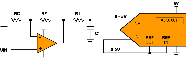
2. I would like to ask the steps to test my ADC which i am using ADS7861 in my case. Do i need to fabricate all my components into PCB board then only i can test for my ADC?Can i just construct a simple circuit that consists only input and output of ADC and test it by applying the varying analog signal and obtaining output using oscilloscope?

3. I failed to obtain any equation of data conversion(analog to digital) from the ADS7861 datasheet. Without the euation, i have no idea how to test the ADC.

  • Hi Ken,

    Actually, it is the CONVST input which is used to trigger the conversion - BUSY is an output indicating the conversion is taking place.  You do not have to use the BUSY line if you don't need/want to.  What BUSY could be used for is as an interrupt to your host processor or FPGA.  Lets say you had a continuous clock rather than the SPI clock you intend to use.  A pulse applied to CONVST would sent the BUSY signal high.  You could then use the falling edge of BUSY to trigger an interrupt and go back to read data after the conversion was complete - in this case, the CONVST and RD signals would need to be separated and you would not be able to run the device at its maximum speed.  To minimize the number of control lines needed, you can run the part as it is depicted in figures 10-13 in the data sheet where RD+CONVST are tied together and chip select can be tied to ground.  You can use an SPI processor with the ADS7861 - and you can potentially use the MOSI output from your processor as a means to control the RD+CONVST, or even the A0 line.  Take a look at the application notes link off of the ADS8361 product folder here (theADS8361 is the 16-bit version of the ADS7861) and you'll find a few ideas on how to wire up the digital side of things.

    To get your VHDL up and running, you could simply wire the digital control lines and tie the analog inputs to a signal generator or other voltage source.  This should get you going there, but would only provide you with enough detail to verify your communication scheme is working.  To see any sort of real performance data from the ADS7861, you are going to need to fabricate the entire circuit.  You may be able to do both with one of our ADS8361 evaluation boards as well.  The ADS7861EVM has connections to all the control pins you'll need.

    Figures 1 through 4 and Table 1 on page 10 of the data sheet provides some details on the ADC's conversion equation.  Your input is +/-Vref, centered on Vref.  A typical single ended input scheme would take the REFOUT voltage and tie it to the (-) input terminal.  That gives you a 0-5V input span on the (+) input terminal when used with the +2.5V internal reference (assumes REFOUT is tied to REFIN).  The LSB size is then max Vin/2^12 or 5V/4096 = 1.22mV.

  • Thank you for your reply,Mr.

    Actually i am first-time user for an ADC and my project requests me to use this ADC. Therefore, i have lot of problem in the design. I hope you can help me and thank you in advanced.

    For the input of ADS7861, i have followed the connection of datasheet that tie REFin and REFout together. According to single-ended input connection, i need to connect the input to a common voltage.For my initial design, i just connect the REFin and REFout only and the input of the ADC is connected to output of my op amp straight away. However, i wonder if i need to connect these two pin together to the (-) input terminal(i use A1 pair in my case, whihch mean the -A1 input pin) in order to get the common voltage after read your reply. My output of op amp i expected to be in the center of 1.5V(Vcenter) and the Vpeak of the analog is varied according to my input of the current transducer. ( motor  -> current transducer -> unity op amp -> ADS7861 -> FPGA -> DSP ). Is it working for my initial design (not using the single ended method provided in datasheet)?


    For the testing, you mean i simply wire the digital control lines and tie the analog inputs to a signal generator or other voltage source. AS i am using only 1 channel, mode 2 which i expect only the data from A1, can i just connect A0 to constant high for A1 channel conversion by ignoring the Chaneel B1 data conversion? Does this will affect the expected result?


  • Hi Ken,

    I've attached a depiction of the typical single ended input scheme.  RG is ‘optional’ and RF could be zero ohms giving you unity gain.  The signal at the +ve input to the ADC would need a CM voltage of +2.5V as depicted in Figure 2 of the data sheet.  If your input signal is going to be Bipolar, you could modify the circuit shown here using additional resistors as shown in Figure 7.  If you only plan on using channel pair A1/B1, you can use Mode II.  If you truly plan on using ONLY channel A1, you can run in Mode I and simply tie the A1 pin high.  You would ignore the SDOB output and leave it open, or terminate it with perhaps a 10K resistor to ground.  For best performance, you should tie the unused analog inputs to the reference as well, do not leave them floating.

  • Thank you for your reply,Mr.

    Now i realised that i should choose the mode 1 instead of mode 2 as the mode 1 can provide me continuous data instead of mixture of data from channel A & B.Thank you for your remind.

    The diagram help me a lot. Thanks.As i am using an unity gain, i should ignore the RG and RF. Since cost stands a role in mark sheet of  my project(i am using SMC), is the R1 necessary ? can i just plug in the capacitor for DC offset removal? Does it affect the result?

    Beside, 1 more main problem i am facing is about the ADC clock. As it mentioned the input clock needed is 16 ^ Fsample and it states Fsample is 500kHz which mean that Fclock is 8MHz, can this be changed? The analog signal that attach from motor before the ADC for my project is around 50/60 Hz only which mean the Fclcok is 800Hz only. Does it affect the whole performance?

    Thank you in advanced.


  • Hi again Ken,

    Take a look at this article http://www.edn.com/contents/images/6447231.pdf as it will explain to you why R1 and C1 should be added to your circuit.  If you choose not to use them, you can simply not populate the components and place a short across R1.

    For the clock, as per the data sheet Timing Specification on page 11, the MAX period shown is the slowest clock frequency that should be applied to the ADS7861 in order to maintain peak performance.  From the table, a 5us period or 200KHz clock is the lower limit for your SCLK.  Having an SCLK of 800Hz would not satisfy the necessary Nyquist-Shannon sampling theorem, at a minimum, you would need to sample your 50/60hz input at 100/120Hz.

  • Good morning,Mr.

    Thanks for your reply. I would try toi increase the signal frequency by applying a crystal oscillator.

  • Good afternoon,mr.  Is me again.

    For the ADS7861, i followed your input design(except that i am using mode2 as i have done my pcb, i just use the existed circuit).

    However, i received no signal from SOA, not even the busy line. I supplied 0.5 and 1MHz to it and i have tried to change the duration between 2 conversion start from 16 clock cycles to 32 clock cycles while A0 remain high. Even all the outputs from FPGA (DE2 board) are the expected value, i cant obtain the SOA . There is no signal from busy (well, actually it got but i think it is internal supply from the ADC as the signal still can be seen even i remove the conversion start signal from FPGA). 

    The signal to the input of ADC is sinewave with 1.4Vpp without offset as the offset will be supplied from the internal reference from ADS7861, is it? Therefore, i think the input is fine for the expected input. Then maybe is my source code that implement the on state of conversion start? As i used 1MHz, it should be 1us for 1 clock cycle. Is it enough to trigger / active the ADC? I am going to test again. Maybe i use 1Hz.


    Thank you in advanced

  • Hi Ken,

    The input signal must be level shifted so that the ADC sees voltage between 0 and 5V at its input pin.  You cannot drive the pin negative.  Pulsing the CONVST should also provide a pulse on the BUSY output pin.  You must also toggle the RD input in order to see serial data on the output pins - serial data will be synchronous to the applied SCLK.  Sixteen clock cycles should be enough to give you a full conversion cycle - 32 won't hurt anything.  Please try to post us a screen shot (o-scope or logic analyzer) of your control lines.

  • Hi,Mr.

    I think i found out the source of my problem.

    Since i am using Alteral FPGA DE2 board, the maximum of the output signal can only up to 3.3V while the ADS7861 need 5V to trigger it.Therefore, i think this is my problem. I didn't convert that to 5V.

    I requested the TXS0108E 8 bit bidirectional voltage-level translator for open-drain and push-pull application. Well, i think i can convert the output signal to 5V, isn't it?

    However, i troubled about the connection of OE(output enable)as it state it need to be connected to ground through a pulldown resistor to avoid damage of the device. At page 13, it state Vcca can greater or equal to Vccb which it wouldn't damage the device during power up sequencing, do i still need to connect it to ground through pulldown resistor (maybe make a switch to change back to high after power up) or can i just connect to Vcc? If i connect to Vcc, would it damage the device?  And since this pin locate at the A side, can i connect to Vcc at A side which i plan to connect to 3.3V.

    P/s: DE2 is 3.3V and i need to convert to 5V for the output signal.Then the A side pins are connected to DE2 board and B side(the Vccb at this side will be connected to 5V at GPIO1/0) which will have the 5V output signal will connect to ADS7861.

  • Hi Ken,

    The pull down is required to keep the output switches from turning on during power up/down of the chip.  I would use the pull down and take the OE pin to a GPIO on your DE2 board.

  • hello,Mr.

    Since i unable to upload the picture that i have capture for the output of result. I have upload it to a forum which link is

    http://www.edaboard.com/ftopic387460.html

    http://www.edaboard.com/ftopic387458.html

    Can you take a look on this. May i know how can i reduce the rise time? Well, it seen like no way to reduce it as i have not connected any resistor and capacitor in between DE2 board and TXS0108E.

    I read that this TXS is only applicable for short trace and without wire/jumper, is it true? Cause i have connected jumper on it.


    the connection: DE2 board --> MC(multi-contact  -60.70001-24-wire, flexi-E from farnell, order code:4326738) --> TXS0108E --> MC wire --> ADS7861


  • May i ask you about the ADS7861. I am facing problem in interfacing with ADC from DE2 board. I used a voltage translator for the conversion of 3.3V to 5 V. The waveform is expected at the output of this translator but problem occurred when i connected to ADC( i supply 2 control signals). I doubt if it is the internal structure of ADC that makes the waveform distorted when 2 signals are transferred. No distortion if only 1 connection is made between ADC and translator but there will be if more than 1 lines are connected. Thus, i doubt if it is the internal structure/ connection has been shorted and this make the signal waveforms mixed (It seen like 2 waveforms are mixed)


    You may refer to these pictures under the links:

    http://rapidshare.com/files/371894736/upload.rar.html.

    P/s : My SPI is 3 control signals (clk, convst and cs) to ADC and 2 signals back to DE2 board(busy and SDO).

  • Ken,

    I am sorry, but we cannot help you debug this 'fly wire' setup using the proto typing vector board.  You must do that on your own.  Please be aware that these experimenter boards can short internally.