This thread has been locked.

If you have a related question, please click the "Ask a related question" button in the top right corner. The newly created question will be automatically linked to this question.

edges on ADS8365 digital control lines

Other Parts Discussed in Thread: ADS8365

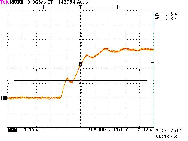
We're using several ADS8365 parts spread across a 15" long board. Unfortunately, the board has been designed with one long trace running between the ADCs for each of the digital side control lines HOLDXn, RDn, A(2:0), etc. Also, no source termination has been implemented on the board. As a result, we're seeing reflections appearing as small discontinuities in the transitions on these signals.

My question is whether these discontinuities are an issue for the ADS8365. We're accessing the ADS8365 channels using direct addressing (rather than the FIFO or cycle modes). My understanding is that this interface for reading sample values is level based and this shouldn't be a problem, but I just wanted to check to be sure.

Thanks

Jeff

  • Hi Jeff!

    Can you post some screen shots of these discontinuities on the ADS8365?  If they are high enough in magnitude to cause a false trigger on HOLDx, RDn or one of the address lines, you could get back some unexpected data.  That would not be an issue for the ADS8365, but it might be for your controller and the equipment you are monitoring.  If there are excursions that exceed the maximum input levels (Vdd +/- 300mV) you could turn on an ESD cell; long term exposure to such transients could cause damage to the device.

  • Hi Tom

    Thanks for the reply. The driver is an FPGA, thru which I'm able to control the slew rate and drive strength. I've experimented a bit to find settings where there isn't any over or undershoot beyond the limits you mentioned. I can't get rid of the double clocking (is that the proper terminology?) in the transition area shown in the scope capture of  HOLDA transition. It looks like I can only make one attachment.... the other control lines and edges  look similar, the discontinuity just occurs at different levels.

    The FPGA has been implemented synchronously, to sample the DATA bus N clocks after HOLDx was driven. So, these double clocks won't affect the FPGA.

    Thanks

    Jeff

  • Hi Jeff,

    I believe everything will be fine, you should not have any issues with that input edge..

  • Excellent. Thanks Tom

  • Hi Tom


    One more follow-on question: is there a minimum slew rate specification for the digital inputs? There's a note on page 12 saying that the timing specs in the table are for inputs with 5 ns rise and fall times, but there's nothing in the datasheet indicating that this is the maximum allowable rise and fall times.

    I can reduce the over and undershoot by decreasing drive strength and slowing down the edges; the cleanest signal transitions are occurring when I have rise/fall times around 5ns or greater.

    thanks

    Jeff

  • Hi Jeff,

    That  note is there to help define the maximum throughput rate of the part.  I don't believe we ever characterized a 'maximum' number for the ADS8365.  As I recall though, the max rise time on SN54/74 CMOS logic devices is ~500 ns, so I suspect this could be a ball park number for you.