


I am currently working in an analog-to-digital converter ADS8332 and have problems with the use of this IC. This IC communicates with the microcontroller over the SPI. I'm a novice in this area and I hope the community can help me.
First, once the configuration of my ADS8332 over the SPI:
I am send for the configuration this hex-stream:
SPI_I2S_SendData16(SPI1, 0xE6FD); /* See Datasheet ADS8332: Give ADS8332 command write into command- and cofiguration register */
/* Write full 16 Bit to adc:
4 Bit CMR (Command register)
0000b: Select analog input channel 0
0001b: Select analog input channel 1
0010b: Select analog input channel 2
0011b: Select analog input channel 3
0100b: Select analog input channel 4
0101b: Select analog input channel 5
0110b: Select analog input channel 6
0111b: Select analog input channel 7
1000b: Reserved
1001b: Reserved
1010b: Reserved
1011b: Wake up
1100b: Read CFR
1101b: Read data
1110b: Write CFR
1111b: Default mode (load CFR with default value)
12 Bit CFR (Configuration register)
Bit 0: Software reset
Bit=0: System reset, returns to "1" automatically
Bit=1: Normal operation
Bit 1: TAG bit output enable
Bit=0: TAG bit output disabled
Bit=1: TAG bit output enable. TAG bits appear after conversion data
Bit 2: Deep Power-Down. This bit set to 1 automatically by wake-up command.
Bit=0: Deep Power-Down enabled
Bit=1: Deep Power-Down diabled (returne normale operation)
Bit 3: Nap Power-Down. This bit set to 1 automatically by wake-up command.
Bit=0: Nap Power-Down enabled
Bit=1: Nap Power-Down diabled (returne normale operation)
Bit 4: Auto-Nap Power-Down enable/disable.
Bit=0: Auto-Nap Power-Down mode enabled (not activated)
Bit=1: Nap Power-Down mode diabled
Bit 5: Pin 10 I/O select for daisy-chain mode operation
Bit=0: Pin 10 is used as CDI input (daisy-chain mode enabled)
Bit=1: Pin 10 is used as EOC/nINT output
Bit 6: Pin 10 I/O function selected when used as an output (EOC/nINT)
Bit=0: Pin used as nINT
Bit=1: Pin used as EOC
Bit 7: Pin 10 polarity select when used as an output (EOC/nINT)
Bit=0: EOC/nINT active high
Bit=1: EOC/nINT active low
Bit 8: Sample rate for Auto-Trigger mode
Bit=0: 500kSPS (21 CCLKs)
Bit=1: 250kSPS (42 CCLKs)
Bit 9: Trigger (conversion start) select: start conversion at the end of sampling
Bit=0: Auto-Trigger: Conversion automatically start three conversion clocks
Bit=1: Manual-Trigger: Conversion manually start on falling edge of nCONVST
Bit 10: Conversion clock (CCLK) source select
Bit=0: Conversion clock (CCLK) = SCLK/2
Bit=1: Conversion clock (CCLK) = internal OSC
Bit 11: Channel select mode
Bit=0: Manual channel select enabled.
Bit=1: Auto channel select enabled.
*/
Then I send to the selection of channel 0 this hex stream:
SPI_I2S_SendData16(SPI1, 0x0000); /* See Datasheet ADS8332: Give ADS8332 command write into command Register "Select analog channel 0" */
Finally, I give the cyclic instructions to send the converted value from channel 0 (See Figure 1):
SPI_I2S_SendData16(SPI1, 0xD000); /* See Datasheet ADS8332: Give ADS8332 command write into command register "Read Data"*/
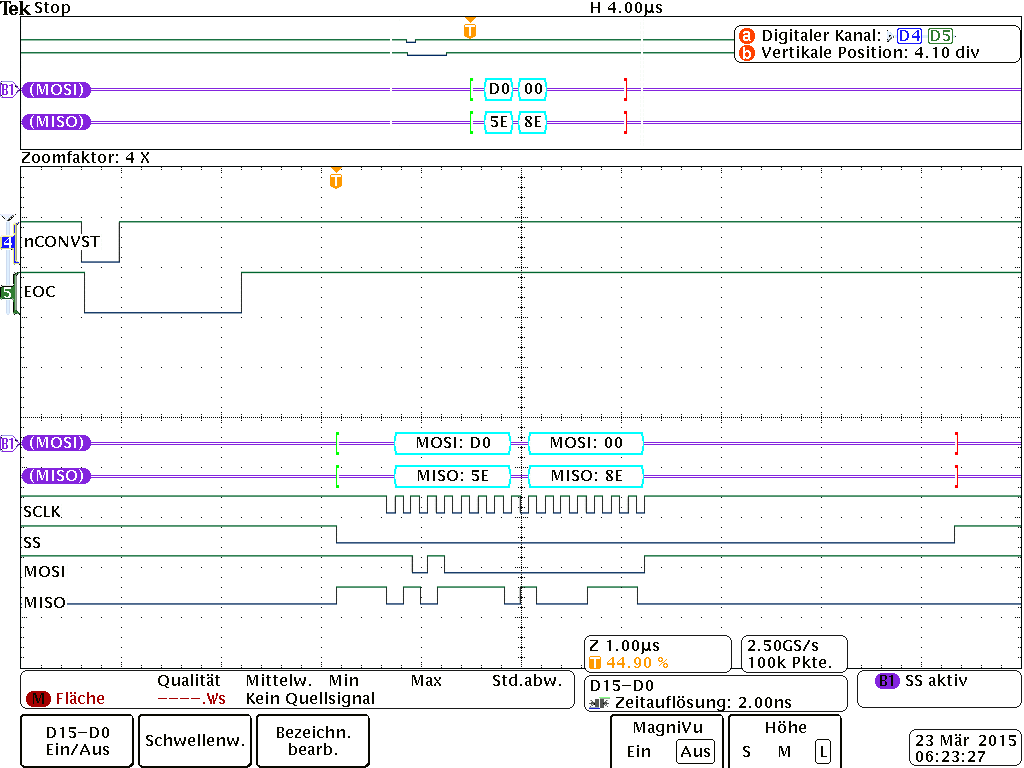
Figure 1: Give ADS8332 command write into command register "Read Data"
My problem is that the MISO signal is always changing, although I always channel 0 query and the channel 0 is connected to a defined voltage potential. The MISO signal is constantly changing and is no proper digital values. I do not know what I'm doing wrong. Please help me...
