This thread has been locked.

If you have a related question, please click the "Ask a related question" button in the top right corner. The newly created question will be automatically linked to this question.

ADS4146 Ground disign question

Other Parts Discussed in Thread: ADS4146

Hi,

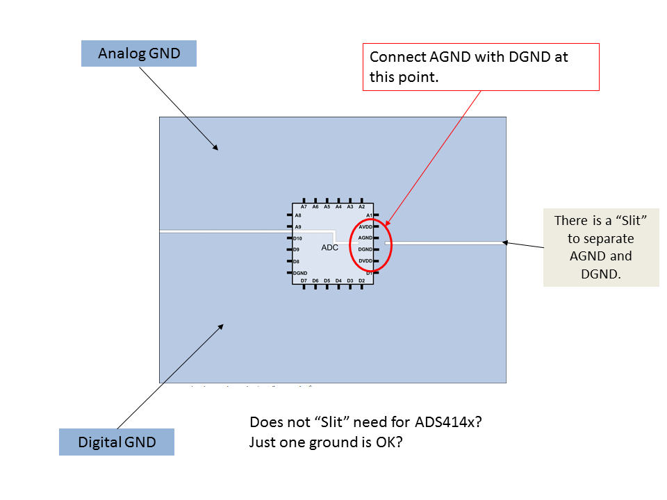
Let me understand the ground plane design about ADS4146.

I found the following E2E conversation.

e2e.ti.com/.../201272

My understanding is,

   Single one grounding is sufficient but sepalated grounding (Analog/Digital) is better than single.

Is this correct?

And is this manner for only ADS41xx? Or is this also available for other high speed ADCs?

Thank you in advance for your advise.

Best Regards,


  • Hi Takumi-san,

    Not correct. We recommend a single ground plane. The recommendation given in that thread was to do the layout with separate ground planes to keep the signals grouped together (all analog with analog, all digital with digital) and then after laying out the signals the ground planes should be reconnected to form a single plane.

    Regards,
    Matt Guibord

  • Hi Matt-san,

    Thank you for your reply!

    Sorry I do not understand well.

    Your idea(Single GND plane) is based on "4 layer" PCB, right? (There is a GND plane independent.)

    In case of "2 layer" PCB, do you think that a slit to sepalate Analog GND and Digital GND is needed?

    I have attached a simple block diagram, could you check it please?

    Best Regards,


  • Hi Takumi-san,

    Just one ground is okay. Do not put a slit in the ground plane.

    Regards,
    Matt Guibord

  • Hi Matt-san,

    Thank you very much for your clear answer !

    I understood.

    Sorry, Could you advise me one more?

    Though I understood that Analog GND and Digital GND should be sepalated, this understanding is not apropriate for high speed ADC.

    Is this correct?

    Or which case should we sepalate the GNDs?

    Best Regards,