This thread has been locked.

If you have a related question, please click the "Ask a related question" button in the top right corner. The newly created question will be automatically linked to this question.

TLV5638, occurring 0V problem!

Other Parts Discussed in Thread: TMS320F28335, TLV5638

I am using TMS320F28335 DSP for motor control.


In this DSP, 4 kHz control rate is implemented by the CPU timer interrupt. And then, SCI (PC to DSP), SPI (for TLV5638), 2 QEP (to obtain motor position) are also implemented in the 4 kHz control rate of the DSP.

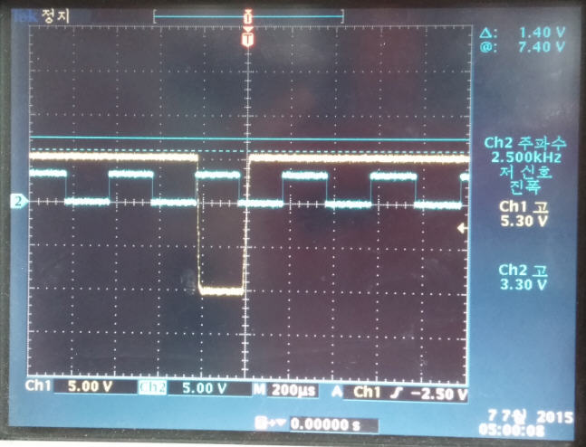
The problem is a DAC function (TLV 5638), sometimes output of the TLV5638 goes to 0 V when two outputs are used.

It seems to be random when i observed this problem.

To solve it, I changed a lot of things such as using external ref. voltage, using external 5V VDD, decrease SPI speed, increase delay time, etc.

Due to these efforts, time interval of 0V problem is reduced, but it is not perfectly solved.

The remain problem is that 0V response still occurred randomly and is about 250 us when the control rate is 4 kHz.

It looks like that sometimes a command (Write data DAC A and update DAC B with BUFFER content) is not working because about 250 us is a period of the 4 kHz control rate.

When i write a command (Write data DAC A and update DAC B with BUFFER content) twice with fast mode/normal operation value, 0V time interval is reduced about 40 us.

About 40 us is my best results. but, still, i did not solve it.

I wonder whether the TLV5638 chip has a flaw or not.

Anyone have an experience of it?

please let me know what do i do to operate TLV5638 perfectly!

Please give me answer  (how to design TLV5638 circuit  and related codes).

I did my best, and  about 40 us  of 0 V   is still remained problem.

p.s>  Why internal ref. voltage occur the problem (similar to shut down of the TLV5638 chip)

Followings are parts of my code.

====================================================================

TLV5638 part

====================================================================

//////// Initialization  (using Ext. rev.  because internal ref.  more aggravate  0V problem.)

// Data is output on falling edge and input on rising edge
SpiaRegs.SPICCR.bit.CLKPOLARITY = 1;

// 16-bit character, Loopback mode Disable (초기값)
SpiaRegs.SPICCR.bit.SPICHAR = 15;

// phase delay
SpiaRegs.SPICTL.bit.CLK_PHASE = 1;

// Master
SpiaRegs.SPICTL.bit.MASTER_SLAVE = 1;

// Enable Transmission
SpiaRegs.SPICTL.bit.TALK = 1;

SpiaRegs.SPIBRR = 23; // Baud rate, 150M/24 = 6.25 Mbps

//////////////////////// Update code

// DAC B: Write data to BUFFER

v->ContRegister = 0x5000; // 0101(2) = Write Data to Buffer


v->DataRegisterB &= 0x0FFF;

v->Output = v->ContRegister | v->DataRegisterB;

while (SpiaRegs.SPISTS.bit.BUFFULL_FLAG);

DELAY_US(DELAY_LENGTH);

// Transmit data to DAC-Buffer
SpiaRegs.SPITXBUF = v->Output;

// Write data to DAC A and update DAC B with BUFFER content
v->ContRegister = 0x8000; // 1000(2) = Write Data to DAC A and Update DAC B with Buffer Content


// 상위 4bit 는 0으로 처리
v->DataRegisterA &= 0x0FFF;

v->Output = v->ContRegister | v->DataRegisterA;


while (SpiaRegs.SPISTS.bit.BUFFULL_FLAG);

// Wait for DAC to finish off
DELAY_US(DELAY_LENGTH);

// Transmit data to DAC-A and update DAC-B with Buffer
SpiaRegs.SPITXBUF = v->Output;


while (SpiaRegs.SPISTS.bit.BUFFULL_FLAG);
// Wait for DAC to finish off
DELAY_US(DELAY_LENGTH);
// Transmit data to DAC-A and update DAC-B with Buffer
SpiaRegs.SPITXBUF = v->Output;

=================================== main.c ===============================================

========= Only show  DAC codes =============================

interrupt void cpu_timer0_isr(void)
{

////////////////////////////////////////////////////////////////////

DAC.DataRegisterA = TestDataA;

DAC.DataRegisterB = TestDataB--;


DAC.update(&DAC);


//////////////////////
PieCtrlRegs.PIEACK.all = PIEACK_GROUP1; // Acknowledge interrupt to PIE
}
//============================================================================================

  • Hi Sehun,

    This is definitely not the expected behavior while using the device.

    Is it possible to share some oscilloscope captures of the digital interface? Ideally of when the output becomes 0 V. If its random it will be difficult to capture for you. Analyzing the SPI interface on the oscilloscope will still be very helpful.


    Also, it it possible for you to share a sample sequence of codes that you are sending to the DAC? This will give me some insight as to what data the DAC has in its registers while trying to update.

  • This is an image which captured from oscilloscope.

    Throughout twice transmission code (Write data to DAC A and update DAC B with BUFFER content), i reduced 0V behavior about 40 us.

    I will reduce SPI speed much more such as  300 kbps  which an example did (found in the internet).  I hope  this approach may solve this problem.

    Nevertheless,  since i am a control engineer student,   i want to know  what a reason of this problem is !!!    

    Someday, i may change a TLV5638 (having the problem) with another TLV5638,   if reduction of the SPI speed do not solve this problem.

    followings are my code which i used.

    ==================================== TLV5638  related ====================================

    #define REF_SEL EXT_REF

    #define DELAY_LENGTH 6L

    //-----------------------------------------------------------------------------
    // TLV5638 API 모듈 정의
    //-----------------------------------------------------------------------------
    typedef struct {
    Uint16 ContRegister; // 4-Bit Control
    Uint16 DataRegisterA; // 12-Bit Data for Channel A
    Uint16 DataRegisterB; // 12-Bit Data for Channel B
    Uint16 Output;
    void (*init)();
    void (*update)();
    } TLV5638;

    ====================================================================================

    //-----------------------------------------------------------------------------
    // TLV5638 API 모듈 함수 정의
    //-----------------------------------------------------------------------------
    void TLV5638_Init(TLV5638 *v)
    {
    // Low-speed Clock 분주비율 설정
    EALLOW;
    SysCtrlRegs.LOSPCP.all = 0x0000; // LSPCLK = SYSCLKOUT
    EDIS;

    // GPIO 54, 55, 56, 57을 SPI 통신용으로 설정
    EALLOW;
    GpioCtrlRegs.GPBPUD.bit.GPIO54 = 0; // Enable pull-up on GPIO54 (SPISIMOA)
    GpioCtrlRegs.GPBPUD.bit.GPIO55 = 0; // Enable pull-up on GPIO55 (SPISOMIA)
    GpioCtrlRegs.GPBPUD.bit.GPIO56 = 0; // Enable pull-up on GPIO56 (SPICLKA)
    GpioCtrlRegs.GPBPUD.bit.GPIO57 = 0; // Enable pull-up on GPIO57 (SPISTEA)

    GpioCtrlRegs.GPBQSEL2.bit.GPIO54 = 3; // Asynchronous input GPIO16 (SPISIMOA)
    GpioCtrlRegs.GPBQSEL2.bit.GPIO55 = 3; // Asynchronous input GPIO17 (SPISOMIA)
    GpioCtrlRegs.GPBQSEL2.bit.GPIO56 = 3; // Asynchronous input GPIO18 (SPICLKA)
    GpioCtrlRegs.GPBQSEL2.bit.GPIO57 = 3; // Asynchronous input GPIO19 (SPISTEA)

    GpioCtrlRegs.GPBMUX2.bit.GPIO54 = 1; // Configure GPIO54 as SPISIMOA
    GpioCtrlRegs.GPBMUX2.bit.GPIO55 = 1; // Configure GPIO55 as SPISOMIA
    GpioCtrlRegs.GPBMUX2.bit.GPIO56 = 1; // Configure GPIO56 as SPICLKA
    GpioCtrlRegs.GPBMUX2.bit.GPIO57 = 1; // Configure GPIO57 as SPISTEA
    EDIS;

    // SPI 통신모듈 초기화
    SpiaRegs.SPICCR.bit.SPISWRESET = 0; // Reset SPI

    // 한번 shift 시 16-bit를 shift 시킴!
    //////////SpiaRegs.SPICCR.all = 0x004F; // Data out on falling edge, 16-bit character, Loopback mode Disable


    ////////////////////////
    /// Note. 1. falling edge without delay (Not Work) (0V 가 자주 발생함)
    /// 2. falling edge with delay (Right choice)
    // 3. rising edge without delay (문제 있음...)
    // 4. rising edge with delay (문제 있음...)


    // Data is output on falling edge and input on rising edge
    SpiaRegs.SPICCR.bit.CLKPOLARITY = 1;

    // 16-bit character, Loopback mode Disable (초기값)
    SpiaRegs.SPICCR.bit.SPICHAR = 15;

    // phase delay
    SpiaRegs.SPICTL.bit.CLK_PHASE = 1;

    // Master
    SpiaRegs.SPICTL.bit.MASTER_SLAVE = 1;

    // Enable Transmission
    SpiaRegs.SPICTL.bit.TALK = 1;


    // SPICLK symmetry 를 위해서는 (SPIBRR + 1) 이 even value 이어야 함.

    //SpiaRegs.SPIBRR = 0x0007; // Baud rate, 150M/8 = 18.75Mbps

    //SpiaRegs.SPIBRR = 0x0009; // Baud rate, 150M/10 = 15 Mbps

    // 11 => 12.5 Mbps (아주 간혹 문제 발생. 5 kHz 일 때)
    //SpiaRegs.SPIBRR = 11; // Baud rate, 150M/12 = 12.5 Mbps

    //SpiaRegs.SPIBRR = 13; // Baud rate, 150M/12 = 12.5 Mbps

    //SpiaRegs.SPIBRR = 15; // Baud rate, 150M/12 = 12.5 Mbps

    //SpiaRegs.SPIBRR = 17; // Baud rate, 150M/12 = 12.5 Mbps

    //SpiaRegs.SPIBRR = 19; // Baud rate, 150M/20 = 7.5 Mbps

    // maybe OK with 6L delay (4 kHz)
    SpiaRegs.SPIBRR = 23; // Baud rate, 150M/24 = 6.25 Mbps


    // 디버깅에서 STOP 이 발생하면, 현재 전송후 정지
    SpiaRegs.SPIPRI.all = 0x0010;

    SpiaRegs.SPICCR.bit.SPISWRESET = 1; // Enable SPI


    // TLV5638 초기화
    v->ContRegister = 0xD000; // 1101(2) = Write Data to Control Register, SPD/PWR = Fast Mode/Normal Operation

    #if(REF_SEL == EXT_REF)
    v->DataRegisterA = 0x0000; // D1/D0 = 00(0) = Set Reference Voltage to External
    #endif

    #if(REF_SEL == INT_REF_2048)
    v->DataRegisterA = 0x0002; // D1/D0 = 10(2) = Set Reference Voltage to 2.048V
    #endif

    #if(REF_SEL == INT_REF_1024)
    v->DataRegisterA = 0x0001; // D1/D0 = 01(1) = Set Reference Voltage to 1.024V
    #endif

    v->Output = v->ContRegister | v->DataRegisterA;

    // ksh 수정

    while (SpiaRegs.SPISTS.bit.BUFFULL_FLAG);

    DELAY_US(DELAY_LENGTH);

    // Transmit FIFO is now empty
    SpiaRegs.SPITXBUF = v->Output;

    // DELAY_US(DELAY_LENGTH);
    //////////////////////////////////
    }

    void TLV5638_Update(TLV5638 *v)
    {
    // DAC A & B 동시 출력

    /////////////////////////////////////////////////////////
    ////////// DAC B Part
    //////////////////////////////////////////////////////////////


    // DAC B: Write data to BUFFER
    // 0001
    //v->ContRegister = 0x1000; // 0001(2) = Write Data to Buffer
    v->ContRegister = 0x5000; // 0101(2) = Write Data to Buffer


    // 상위 4비트는 0 으로 만들기.
    //v->DataRegisterB = v->DataRegisterB & 0x0FFF;
    v->DataRegisterB &= 0x0FFF;

    v->Output = v->ContRegister | v->DataRegisterB;

    //while (SpiaRegs.SPIFFTX.bit.TXFFST != 0);
    while (SpiaRegs.SPISTS.bit.BUFFULL_FLAG);

    DELAY_US(DELAY_LENGTH);
    //DELAY_US(3);

    // Transmit data to DAC-Buffer
    SpiaRegs.SPITXBUF = v->Output;


    ////////////////////////////////////////////////////////////////
    //////// DAC A Part (A & B 동시 갱신)
    ////////////////////////////////////////////////////////////////

    // Write data to DAC A and update DAC B with BUFFER content
    // 1000
    v->ContRegister = 0x8000; // 1000(2) = Write Data to DAC A and Update DAC B with Buffer Content
    //v->ContRegister = 0xC000; // 1100(2) = Write Data to DAC A and Update DAC B with Buffer Content


    // 상위 4bit 는 0으로 처리
    v->DataRegisterA &= 0x0FFF;

    v->Output = v->ContRegister | v->DataRegisterA;


    while (SpiaRegs.SPISTS.bit.BUFFULL_FLAG);

    // Wait for DAC to finish off
    DELAY_US(DELAY_LENGTH);

    // Transmit data to DAC-A and update DAC-B with Buffer
    SpiaRegs.SPITXBUF = v->Output;

    while (SpiaRegs.SPISTS.bit.BUFFULL_FLAG);
    // Wait for DAC to finish off
    DELAY_US(DELAY_LENGTH);
    //DELAY_US(3);
    // Transmit data to DAC-A and update DAC-B with Buffer
    SpiaRegs.SPITXBUF = v->Output;

    }

    =========================== main.c ==============================================

    ===============================================================================


    void main(void)
    {

    //============================================================================================
    // Step 1. Disable Global Interrupt
    // 전역 인터럽트 비-활성화 및 인터럽트 플래그 초기화
    //--------------------------------------------------------------------------------------------
    // Disable CPU interrupts
    DINT;

    // Disable CPU interrupts and clear all CPU interrupt flags
    IER = 0x0000;
    IFR = 0x0000;
    //============================================================================================


    //============================================================================================
    // Step 2. 시스템 컨트롤 초기화:
    //--------------------------------------------------------------------------------------------
    // 초기화 시작
    // PLL, WatchDog, enable Peripheral 클럭의 초기화
    // DSP280x_SysCtrl.c 에 정의된 함수.
    // 2.1 Disables the watchdog
    // 2.2 Set the PLLCR for proper SYSCLKOUT frequency
    // 2.3 Set the pre-scaler for the high and low frequency peripheral clocks
    // 2.4 Enable the clocks to the peripherals
    //--------------------------------------------------------------------------------------------
    InitSysCtrl();
    //============================================================================================


    //============================================================================================
    // Step 3. 인터럽트 초기화 (DSP2833x_PieCtrl.c / DSP2833x_PieVect.c 파일 참조)
    //--------------------------------------------------------------------------------------------
    InitPieCtrl();

    InitPieVectTable();

    // Vector Remapping
    EALLOW;
    PieVectTable.TINT0 = &cpu_timer0_isr;


    // SCI-A 수신 인터럽트 함수 리매핑
    //PieVectTable.SCIRXINTA = &sciaRxIsr;
    PieVectTable.SCIRXINTA = &sciaRxFifoIsr;

    EDIS;
    //============================================================================================


    //============================================================================================
    // Step 4. GPIO 초기화
    //--------------------------------------------------------------------------------------------
    EALLOW;
    // For LED indicators
    GpioCtrlRegs.GPAMUX1.all = 0x00000000; // 모두 GPIO 모드로 설정. GPIO A Mux 2 Register (GPIO16 to 31)
    GpioCtrlRegs.GPADIR.all = 0x00F00000; // GPIO 20 ~ 23 outputs (출력)으로 설정
    GpioDataRegs.GPADAT.all = 0x00F00000; // GPIO 20 ~ 23 출력 High

    /////////////////////////////////////////////////////////////////////////////////////////////

    // for EQEP A
    GpioCtrlRegs.GPBPUD.bit.GPIO50 = 0; // Enable pull-up on GPIO50 (EQEP1A) //
    GpioCtrlRegs.GPBPUD.bit.GPIO51 = 0; // Enable pull-up on GPIO51 (EQEP1B) //
    // GpioCtrlRegs.GPBPUD.bit.GPIO52 = 0; // Enable pull-up on GPIO52 (EQEP1S) //
    // GpioCtrlRegs.GPBPUD.bit.GPIO53 = 0; // Enable pull-up on GPIO53 (EQEP1I) //

    GpioCtrlRegs.GPBCTRL.bit.QUALPRD2 = 0x00; // Specifies the qualification sampling period for GPIO48 to GPIO55 //

    GpioCtrlRegs.GPBQSEL2.bit.GPIO50 = 0; // Sync to SYSCLKOUT GPIO50 (EQEP1A)

    GpioCtrlRegs.GPBQSEL2.bit.GPIO51 = 0; // Sync to SYSCLKOUT GPIO51 (EQEP1B)


    // Select the pin function: (GPxMUXn registers 구성)
    // sprufb0d - 76 page 참고
    GpioCtrlRegs.GPBMUX2.bit.GPIO50 = 1; // Configure GPIO50 as EQEP1A //
    GpioCtrlRegs.GPBMUX2.bit.GPIO51 = 1; // Configure GPIO51 as EQEP1B //
    // GpioCtrlRegs.GPBMUX2.bit.GPIO52 = 1; // Configure GPIO52 as EQEP1S //
    // GpioCtrlRegs.GPBMUX2.bit.GPIO53 = 1; // Configure GPIO53 as EQEP1I //

    // for EQEP B
    GpioCtrlRegs.GPAPUD.bit.GPIO24 = 0; // Enable pull-up on GPIO50 (EQEP1A) //
    GpioCtrlRegs.GPAPUD.bit.GPIO25 = 0; // Enable pull-up on GPIO51 (EQEP1B) //

    GpioCtrlRegs.GPACTRL.bit.QUALPRD3 = 0x00; // Specifies the qualification sampling period for GPIO 24 to GPIO 31 //
    GpioCtrlRegs.GPAQSEL2.bit.GPIO24 = 0; // Sync to SYSCLKOUT GPIO50 (EQEP1A)
    GpioCtrlRegs.GPAQSEL2.bit.GPIO25 = 0; // Sync to SYSCLKOUT GPIO51 (EQEP1B)

    // Select the pin function: (GPxMUXn registers 구성)
    // sprufb0d - 76 page 참고
    GpioCtrlRegs.GPAMUX2.bit.GPIO24 = 2; // Configure GPIO50 as EQEP1A //
    GpioCtrlRegs.GPAMUX2.bit.GPIO25 = 2; // Configure GPIO51 as EQEP1B //

    EDIS;


    //============================================================================================
    // Step 4. Initialize Application Variables
    //--------------------------------------------------------------------------------------------

    ////////////////////////////////////////
    // SCI communication initilize통신 관련

    /////////////////////////////////////////
    ///////// DAC (TLV5638) 관련
    ///////////////////////////////////////
    BackTicker = 0;

    TestDataA = 3200;
    TestDataB = 0x0FFF;

    DAC.init(&DAC);

    ////////////////////////////////////////
    //// EQEP 관련
    ////////////////////////////////////////////
    // EQEP

    /////////////////////////

    //============================================================================================

    //============================================================================================
    // Step 3. SCI setting
    //--------------------------------------------------------------------------------------------
    InitSciaGpio();

    /* SCI 모듈 설정 */
    SciaRegs.SCICTL1.bit.SWRESET = 0; // All affected logic is held in the specified reset state until a 1 is written to SW RESET.
    // SCI CHAR2-0 Bit: Character length (Bits): 8 bits
    SciaRegs.SCICCR.all = 0x07; // 0x07 = 0000 0111
    // TXEBA: Transmitter enabled, RXEBA: Send received characters to SCIRXEMU and SCIRXBUF
    SciaRegs.SCICTL1.all = 0x03; // 0x03 = 0000 0011

    // LOSCLK = 150 MHz 로 고려해서 Baud Rate 다시 계산.
    ///////// 38400 bps 설정 (487 (1E7h) BRR): 0.06 % Error at 150 MHz
    /// BRR: 0x1E7
    SciaRegs.SCIHBAUD = 0x01;
    SciaRegs.SCILBAUD = 0xE7;

    // SCI의 송신 FIFO 설정

    SciaRegs.SCIFFTX.bit.SCIFFENA = 1; // SCI FIFO 사용 설정 Enable
    SciaRegs.SCIFFTX.bit.TXFIFOXRESET = 1; // SCI 송신 FIFO RE-enable

    // SCI의 수신 FIFO 설정 with 인터럽트
    SciaRegs.SCIFFRX.bit.RXFFINTCLR = 1; // SCI 수신 FIFO 인터럽트 플래그 클리어
    SciaRegs.SCIFFRX.bit.RXFIFORESET = 1; // SCI 수신 FIFO RE-enable
    SciaRegs.SCIFFRX.bit.RXFFIENA = 1; // SCI 수신 FIFO 인터럽트 Enable
    SciaRegs.SCIFFRX.bit.RXFFIL = 16; // SCI 수신 FIFO 인터럽트 레벨 설정 (16개 data가 입력되면 수신 인터럽트 수행)


    SciaRegs.SCICTL1.bit.SWRESET = 1; // After a system reset, re-enable the SCI by writing a 1 to this bit.


    PieCtrlRegs.PIEIER9.bit.INTx1 = 1; // PIE 인터럽트(SCIRXINTA) : Enable
    IER |= M_INT9;

    //============================================================================================

    //============================================================================================
    /*-----------------------------------------------------------------------------
    Step 7
    7.1 Initialize Periphrals for User Application
    -----------------------------------------------------------------------------*/
    /* Initialize Enhanced QEP Module 1 */
    InitEQep1(PositionMax);

    /* Initialize Enhanced QEP Module 2 */
    InitEQep2(PositionMax);


    //============================================================================================
    // Step 5. CPU Timer 초기화 (제어 주기 관련)
    //--------------------------------------------------------------------------------------------

    // CPU Timer 초기화
    InitCpuTimers();

    Cpu_Clk = 150; // 현재 시스템 클럭을 설정 (MHz 단위)

    // 4 kHz => 0.25 ms = 250 us
    Timer_Prd = CONTROL_RATE; // 타이머 주기 설정 (usec 단위)

    // CPU Timer0 을 0.25 밀리초 주기로 설정
    ConfigCpuTimer(&CpuTimer0, Cpu_Clk, Timer_Prd);

    // CPU Timer0 시작
    StartCpuTimer0();

    // CPU Timer0 인터럽트 활성화
    PieCtrlRegs.PIEIER1.bit.INTx7 = 1; // PIE 인터럽트(TINT0) 활성화
    IER |= M_INT1; // CPU 인터럽트(INT1) 활성화

    //============================================================================================

    //============================================================================================
    // Enable global Interrupts and higher priority real-time debug events:
    //--------------------------------------------------------------------------------------------
    EINT; // Enable Global interrupt INTM
    ERTM; // Enable Global realtime interrupt DBGM
    //============================================================================================


    //============================================================================================
    // IDLE loop. Just sit and loop forever :
    //--------------------------------------------------------------------------------------------
    while(1)
    {
    Loop_cnt++;


    }
    //============================================================================================

    }
    //============================================================================================
    // 메인 함수 - 끝
    //============================================================================================

    //============================================================================================
    // 인터럽트 서비스 루틴 정의
    //--------------------------------------------------------------------------------------------
    interrupt void cpu_timer0_isr(void)
    {
    GpioDataRegs.GPATOGGLE.all = 0x00F00000; // LED 토글

    CPU_Timer0_Isr_cnt++;

    Timer_pulse = !Timer_pulse;

    ////////////////////////////////////////////////////////////////////

    BackTicker++;

    SCI_cnt++;


    ///////////////////////////////////////////////////////
    ///// EQEP 1, 2
    //////////////////////////////////////////////////////////
    ///////////////////
    // EQEP A
    // Check Position & Direction //

    //

    //

    //

    // Finally, calculate positions

    fCurrentPos[0] = RotateAngleDegree[0] + 360.0*NumOfTurns[0];


    // EQEP B
    // Check Position & Direction

    // Finally, calculate positions
    fCurrentPos[1] = RotateAngleDegree[1] + 360.0*NumOfTurns[1];


    ///////////////////////////////////////////////////////////////
    ///////// DAC (TLV5638)
    ///////////////////////////////////////////////////////////////

    // 12 bit DAC

    // Test code

    DAC.DataRegisterA = TestDataA;

    DAC.DataRegisterB = TestDataB--;


    DAC.update(&DAC);

    //////////////////////////////// SCI comm. code ////////////////////////////////////////////////

    //---------------------------------------------------------------------------
    // A. SCI 데이터 송신
    // ---------------------------------------------------------------------------//
    // Trnasmit FIFO가 empty 가 될때까지, 대기!
    while(SciaRegs.SCIFFTX.bit.TXFFST != 0);

    // Transmit FIFO 가 empty 이면, 송신을 수행한다.

    for(i=0;i<RxFifoLevel;i++)
    {
    SciaRegs.SCITXBUF = TxBuff[i] & 0x00FF;
    }

    // SCI 통신 if 문 End
    ///////////////////////////////////////////////////////
    }

    //////////////////////
    PieCtrlRegs.PIEACK.all = PIEACK_GROUP1; // Acknowledge interrupt to PIE
    }
    //============================================================================================

  • Until now, i used DSP's SPI funciton (SPISIMOA, SPICLKA, SPISTEA).


    Refer to a document (academic.cankaya.edu.tr/.../Module7.pdf)


    I changed a SPISTEA pin as a GPIO output pin. Then, i give a /CS signal manually (like the above document.).


    Now, it seems to be DAC output ok.

    Maybe i should observe the DAC output signal very long time so that the 0V problem is really solved or not.

    (The frequency of 0V problem is decreased, but 0V problems are still occurred occasionally and unexpectedly.)


    Several things i have questions.

    1. power supply for the TLV5638.

    I purchased 28335 module from the company in korea and when 5V (from the 5V output with 3A DC adapter which also provide DSP module power) is connected to TLV5638, 0V problem occurred. Thus, I am using DC power supply device now.

    I wonder why 5V in the DSP module cause the problem? It is very curious to me.


    2. Delay time for SPI comm.

    In the above reference doc. (academic.cankaya.edu.tr/.../Module7.pdf)

    They used a following delay function.

    for (SPI_i=0; SPI_i < 100; SPI_i++);


    When I tested it with various delay time, delay time is sensitive to 0V problem (maybe SPI comm. or TLV5638 update problems.)

    Please give me advise how to design or calculate proper delay time in order to operate TLV5638 well (with respect to SPI speed, etc).

  • Hi Sehun,

    Thank you for providing all of this information. I cannot verify the validity and accuracy of the document you quote.

    Can you share an oscilloscope capture of DIN and SCLK?

    Do you notice the a voltage drop on VREF during the output droop?