This thread has been locked.

If you have a related question, please click the "Ask a related question" button in the top right corner. The newly created question will be automatically linked to this question.

Driving ADS8332

Other Parts Discussed in Thread: ADS8332, AM3357, PGA204, PGA206, PGA205, OPA192, INA114, OPA320

Hi,


I am planning to use two ADS8332 to sample a total of 16 single-ended channels and  I have a few questions before I select the ADC.

  • Sitara AM3357 will be used as the cpu
  • The two ADCs will likely be on the same (dedicated) SPI bus. Likely wired in daisy chain mode
  • I need at least a 10kHz sampling rate for all channels. A quick calculation shows this should be possible (500ksps/16ch = 31ksps/ch).
  • The input channels will be driven by an instrumentation amplifier (PGA204, PGA206)

My questions are as such:

The Driver Amplifier Choice section of the ADS8332 datasheet shows an op-amp driving the ADC. Can I drive the ADC input using the output of the the instrumentation amplifiers (without the op-amp)?

How can I determine a realistic sampling rate for two devices? In Table 3, Auto-trigger mode takes 21CCLKs for each conversion. however, I am not sure how much overhead is required for the communication

  • Hi Igor,

    The driving amplifier needs has to have enough bandwidth and low enough output impedance over frequency to be able to charge the internal sampling capacitor and settle within the 16 bit resolution. Since the PGA205/4 are instrumentation amplifiers, the BW is limited and dependent in gain setting, and therefore, they need to be buffered prior driving the SAR ADC. 

    One possibility is to place a buffer between the MUXOUT and ADCIN pins.  Are you using +/-15V supplies in the system for the PGA's?  Are you planning to use VREF=2.5V or VREF=4.096V?  I will look into providing a suggestion for the driver and RC filter.  A possibility may be the OPA192, offering very good DC performance,

    Regarding the daisy chain data rate for two devices, the device allows you to use either the internal or external conversion clock (CCLK). 

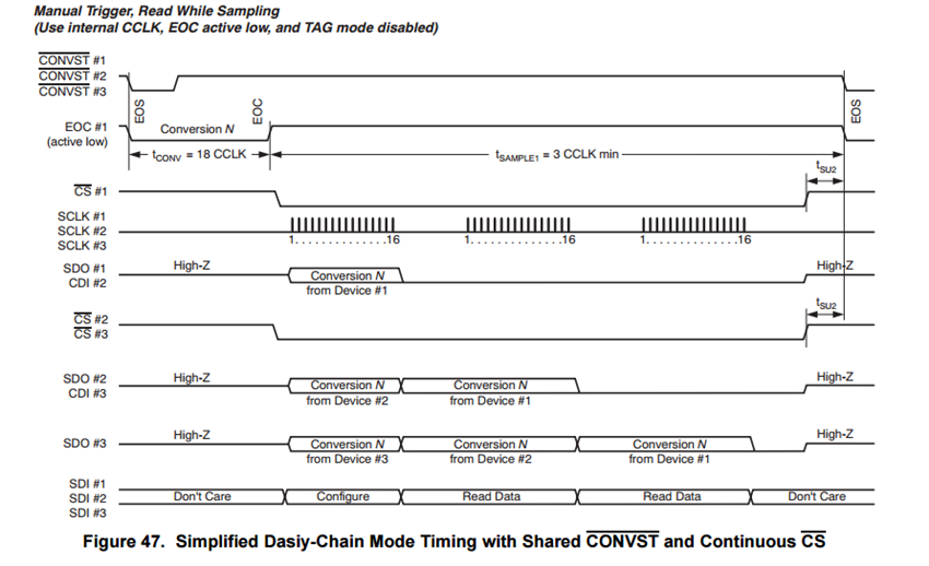
    For example, when using (2) ADS8332 in Daisy Chain mode with SCLK both as I/O and Conversion Clock, manual trigger, looking at Figure 47 with simplified daisy-chain mode with shared CONVST, one transaction to read one set of conversions from ADC#1 and ADC#2 will require:

    18 CCLKs (18x2=36 SCLKs) for conversion time + 16 SCLK's for ADC #2 + 16 SCLKs for ADC#1 + tsu2

    Assuming SCLK=21MHz max; this will yield allow you to trigger a conversion in both channels every 68 SCLKs+20ns, or 3.26uS.  Each ADC is running at ~307KSPS.  This will allow you to scan all 16 channels every 3.26uS*8=~26uS, or allow you an effective rate of 307kSPS/8= ~38kSPS per channel (since both ADC'#1 and ADC#2 are converting simultaneously),

    Please see below similar example with (3) devices in daisy chain mode.

    I will provide more detailed feedback on the amplifier driver example in the next couple of days.

    Best Regards,

    Luis


  • Hi Luis,
    Thank you for your reply.

    I plan to power the PGA's using -1.8/+32V. We need to handle large common mode voltages and using ground as the reference simplifies the design. Our previous design used INA114 and a different SAR DAC with a 2.5V reference. In this spin of the design I will be using a 4V reference.

    Placing a buffer between the MUX and the ADC seems like a good solution, it would save some real estate on the board.

    As for the ADC communication, it may be better if I place each ADC on it's own bus. That way the SPI peripheral can handle all communication without taxing the CPU.

    Regard,
    Igor
  • Hi Igor,

    Placing the buffer between the MUXOUT and ADCIN should work well for you.  

    For example, using  a single OPA320 as a buffer (in the non-inverting configuration, G=1) between MUXOUT and ADCIN, with a low pass filter, R= 30Ohms, C=1nF infront of the OPA320 will settle within less than 1/2 LSB error in less than <700nS.  If the ADS8332 is used in manual trigger mode, with internal conversion clock, and allowing a 785nS sampling time (tsample), the circuit will support a ADC data rate up to ~400kSPS; or 400kSPS/8=50kSPS per channel.

    Thank you and Best Regards,

    Luis