This thread has been locked.

If you have a related question, please click the "Ask a related question" button in the top right corner. The newly created question will be automatically linked to this question.

Voltage Reference of multi-ADS1281

Other Parts Discussed in Thread: ADS1281, REF5020, REF5025, OPA735, REF5050, OPA227, OPA313, THS4531, TINA-TI

Hi,

I want to design a 8-channels recorder. 

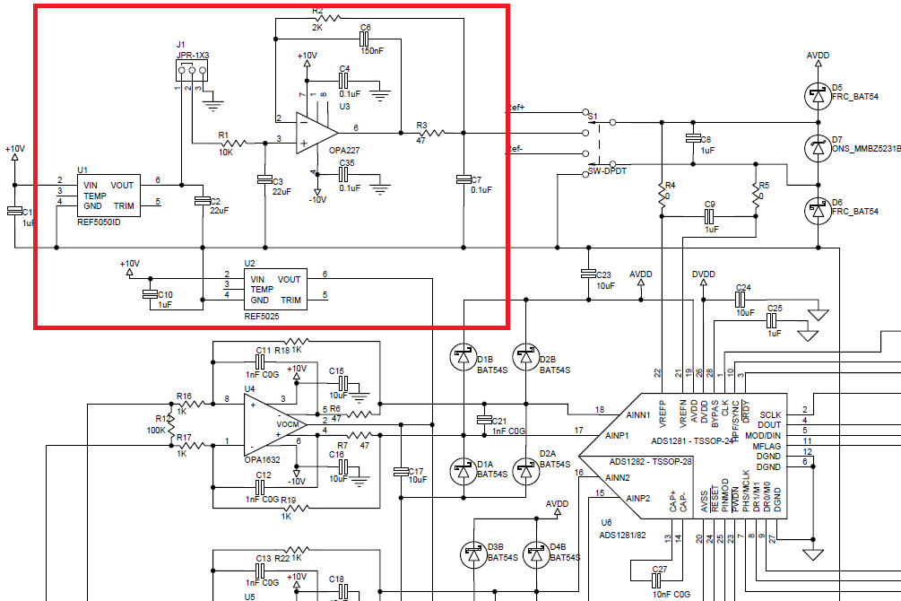
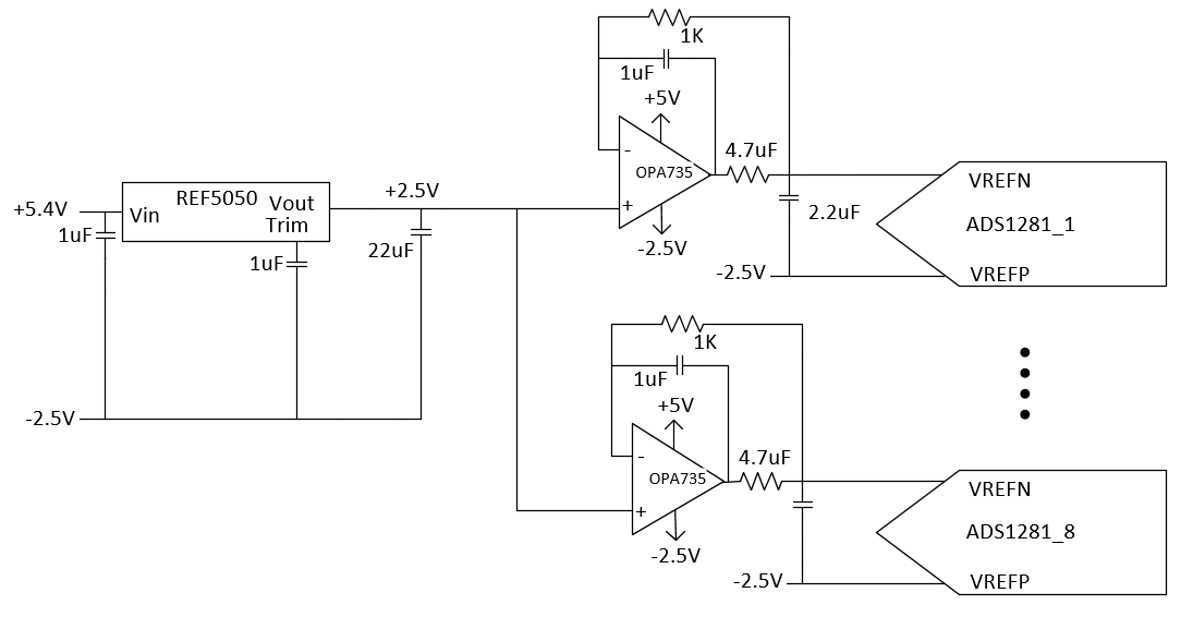
I use eight ADS1281 ADCs for synchronized.

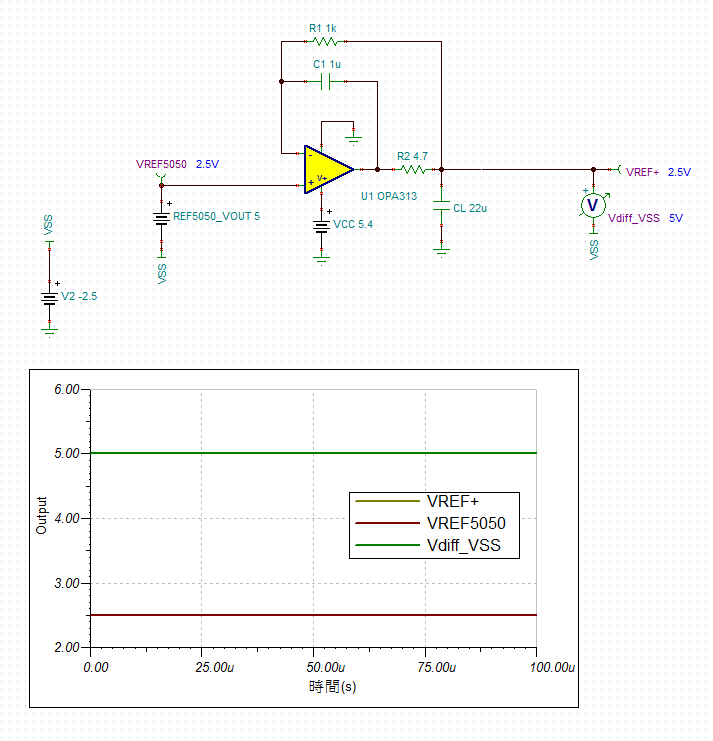
The Vref design is from the datasheet of REF50xx which is shown in the following figure.

(The circuit is REF5020, and I will replace it with REF5025)

*There are eight ADS1281, but only four ADS1281 are drawn)

My question is...

Can I use only one REF5025 for the VREF of eight ADCs?

I am not sure the performance of the circuit.

Hope someone can help me. Thanks

YHH

  • Hi Yu-Hung,

    I know that the REF50xx should be able to drive at least four ADS1281's; however, I have not tried it with eight ADCs. Let me get back to you on that point. I'll see if I can simulate this case.

    Regarding the circuit diagram, I would recommend removing the OPA735 and connecting the REF50xx's "GND" pin directly to the ADS1281's AVSS pin. Then I would use a REF5050 to generate a 5V reference without the need for the op amp. This would improve performance by removing the op amp circuit's noise, offset, and drift contribution to the reference voltage! (...I'm assuming you're operating the ADS1281 off of a +/-2.5V bipolar supply, so...) You would another supply rail (>3V) to power the REF5050.

    Best Regards,
    Chris

  • Hi Chris,

    Thank you, waiting for your simulation. :)

    I know what you say about REF5050.
    The reference circuit can be found in the datasheet of ADS1281EVM.
    It seems that
    1. Vref- = -2.5V(AVSS),
    2. Vref+ = -2.5V(AVSS) + 5V(REF5050), and
    3. 0V(VOCM of A/D pre-amp) = -2.5V(AVSS) + 2.5V(REF5025).

    But it also has an OPA227, I guess it is used for LPF.

    Regards,
    YHH

  • Hi Yu-Hung,

    Thanks for your patience!

    After running some simulations, I think you'll get the best performance by buffering each ADC's reference input. You can use a single REF5025, but the 8 op amps are required to prevent cross-talk errors between the ADC reference inputs. It is very likely that the case with only 4x ADS1281's would also benefit from the added buffers.

    I tried to find a low-power solution for you that provided good performance and I found the OPA313 reference buffer circuit described in this TI Design:

    Unfortunately I cannot share the ADS1281 reference model, but here are my simulation results:

    The simplified ADS1281 reference input is a switched-capacitor circuit (the actual model is more complex). When this capacitor samples the reference voltage it must charge up within the sampling time.

    There are two things to notice:

    1. When this sampling process starts, the OPA313's output voltage initially droops until the op amp is able to recover. This takes about 5ms. Therefore, conversion results during this time may need to be ignored, because they will have a higher than normal gain error associated with this drop in reference voltage.
    2. The voltage on the sampling cap settles to within 1uV of it's final value (when compared to the DC steady state voltage seen by this cap when the circuit is not switching). The resulting gain error is then 1,000,000 * (1uV / 2.5V) = 0.4 ppm, which is less than the ADS1281's gain error after calibration (about 2 ppm).

    I hope this helps give you a starting point with your system design. Let me know if have additional questions!

    Best Regards,
    Chris

  • Hi Chris,

    Thanks for your simulation.

    Base on your suggestion, here is my design.

    I will use only one power pack for all devices include the sensor.

    As you said, the VREF circuit is shown as following.

    But the power supply range of OPA313 is 5.5V, so it can not use for REF5050.(I need +/- 2.5V)

    THS4531 is used for single-end input to differential output which is in the datasheet (Figure 74. Differential Input to Differential Output Amplifier). 

    Should I use 8 op amps for Vocm on one REF5025?

    Or Vocm connects to ground directly?

    Thank you very much for your doing.

    Have a nice weekend.

    Regards,

    Yu-Hung

  • Although the gain is 0.2 V/V, but the sensor output range(+/-10V) is higher than power supply of THS4531(+/- 2.5V).

    Does it effect the performance?

  • Hi Yu-Hung,

    When I ran the simulation with the THS4531 I looked at the voltages at the input pins...even though you're applying a +/-12V signal, the voltage at the THS4531 input pin is attenuated by the feedback resistor network, as shown below:

    I know you're concerned about the power consumption; therefore, you may want to increase the size of the feedback resistors. Currently, with the 1k and 200 Ohm resistors there will be an 11mA current flowing from the sensor output, through the feedback resistor network, and sinked by the THS4531.


    Regarding the OPA313, you could connect the OPA313's negative supply to ground and power it from either a 3.3V or 5V supply rail. The 2.5V output from the REF5050 (referenced to AVSS = -2.5V) would be within the op amps common-mode input range. I don't know what the output impedance of the OPA735 looks like compared to the OPA313; therefore, you may need to modify the compensation from the OPA313 circuit.

    Best Regards,
    Chris

  • Hi Chris,

    You are right!!

    I will increase the value of resistors of THS4531, maybe 20k and 4k.

    I modify the OPA313 TINA-TI Reference Design (Simulation Models) as below.

    The output voltage(VREF+) is 2.5V.

    I will try to layout a demo board to test.

    Hope everything works well. ^_^

    BTW, does TINA-TI support IBIS model now?

    There is a IBIS model in ADS1281 page, but the forum thread(3 years ago) said not support.

    Thanks again, Chris.

    Regards,

    Yu-Hung

  • Here is my design which the sampling rate is 250SPS.

    AVDD=+2.5V, AVSS=-2.5V

    V1IN+  -  V1IN- = +/- 10V. (reference to GND)

    V2IN+  -  V2IN- = +/- 10V. (reference to GND)

    There is a VREF buffer(OPA313) for each ADS1281.

    I have ever seen that RFI filter place before and after THS4531.

    In general, which one is better?

    Regards,

    Yu-Hung

  • Hi Yu-Hung,

    IBIS models are mainly used for verifying digital signal integrity. I don't think TINA supports them. Usually the PCB design suites will have tools that make use of IBIS models (such as Mentor Graphics HyperLynx). I haven't used these tools much myself.

    Regarding your schematic...
    - Make sure you connect the "GND" pin of the REF5050 and REF5025 to AVSS
    - I'd also recommend connecting "VREFN" from the ADS1281 to the REF5050's GND pin with a trace. This is a layout recommendation, not a problem with the schematic. This type of connection reduces the noise seen by the "VREFN" pin.
    - You could place filters (you called it an RFI filter) before and after the THS4531, it would depend on what you want to accomplish with them. For RFI filtering, I would place these BEFORE the THS4531. A filter after the THS4531 would usually be more intended for anti-aliasing filtering.
    - (I assume you'll finish adding the missing ADS1281 connections, but that they weren't needed for your question.)

    Best Regards,
    Chris
  • Hi Chris,

    Yes, the "GND" pin of the REF5050 and REF5025 should be connect to AVSS.

    I missed that.

    The only one I would like to know is the Vocm side.

    Should I put a voltage follower or reference buffer(like VREFP) BEFORE each "Vocm" pin of THS4531?

    Regards,

    Yu-Hung Hsiao

  • Hi Yu-Hung,

    No, you shouldn't need a buffer for the VOCM input. In fact, you could probably leave the VOCM pin floating, because the THS4531 will internally set VOCM to a mid-supply voltage (see page 33 of the THS4531 data sheet) . In your circuit, the REF5025 output and the THS4531 mid-supply voltage are approximately the same, and I don't see much benefit from driving this pin. However, I would add the 0.22uF cap (also shown in the datasheet) from VOCM to AVSS to provide some noise filtering on this signal.

    Best Regards,
    Chris

  • Hi Chris,

    Thanks for your guidance.

    I will remove REF5025 and put a 0.22uF cap in Vocm pin.

    Thank you again. :)

    Regards,

    Yu-Hung