This thread has been locked.

If you have a related question, please click the "Ask a related question" button in the top right corner. The newly created question will be automatically linked to this question.

Using Vcm on VCA2617 for input CM bias

Other Parts Discussed in Thread: VCA2615, VCA2617, TINA-TI

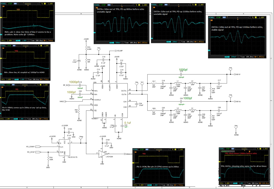
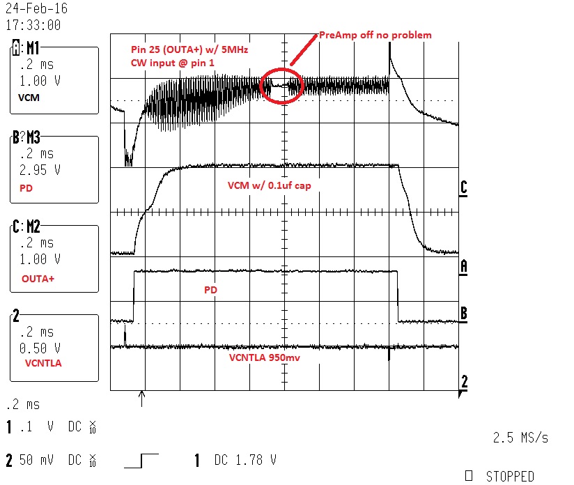
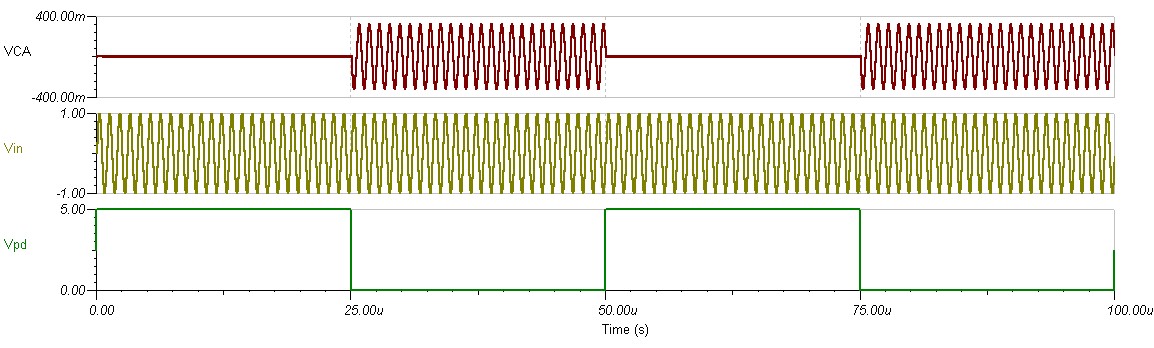
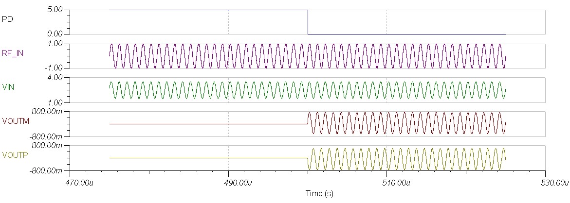
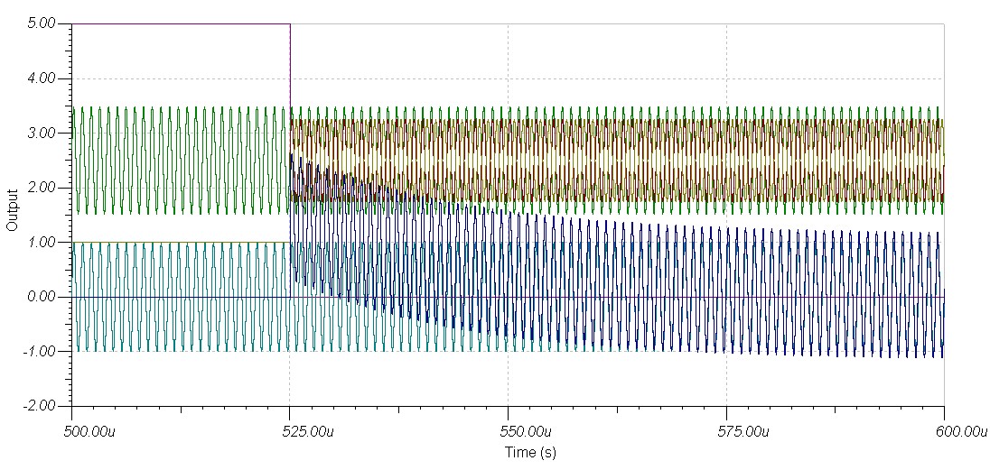
The AC coupled input pin (0.01uf) is VERY slow to come up after ~PD comes up. The 300k input resistance makes this so.

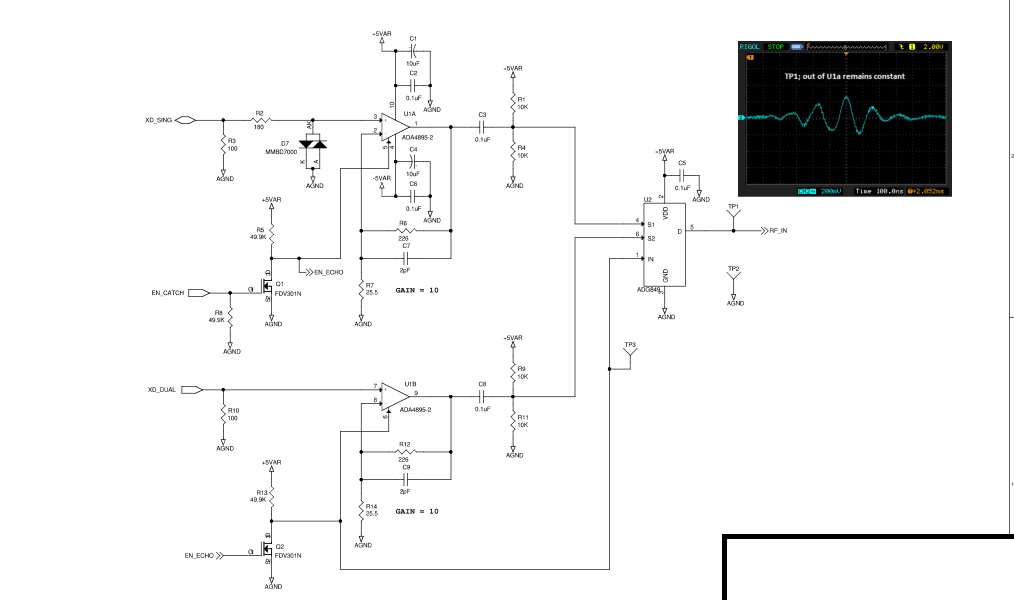
Can Vcm  (pin 5) be used to bias this to the internal CM voltage?

What is the impedance of this output of the VCA2617? In the VCA2615 data sheet, Figure 58 shows Vcm used to bias a MUX but no values are given for this part. Is the VCA2617 the same and what values can we use to bias the input pin?

The goal is to get the Power-Up Response Time, through an AC coupled signal, close to the spec'd 25us.

Thanks!

Jesse

  • Jesse,

    We have received your post and hope to have a response back to you soon.
  • Schematics of VCA2617 with 1.3s up time from ~PD.

  • Jesse,

    The VCA2615 and VCA2617 are very similar. You can use the same application given on Figure 58 of the datasheet as you referenced. The reason no values were given was because this was an example circuit and as long as the CM is in the range of 1.85V to 3.15V it should work.

  • Amy, Thank you.
    On our proto board we are proposing to:
    Since we are using a single ended input, take C22 out and let INA- float
    Remove our 2.5v bias: take ot R1 and the GND at R4
    Connect Vcm through the 2K at R4 to the input of U2.
    Short the 1000pf at C18.
    So, Vcm is driving the 1000pf C3 and the 300k 2617 input through a 2k resistor.
    Will this work?
    Is there a test schematic for developing the specs for either the 2617 or 2615?
    I noticed that there is a POWER UP/DOWN RESPONSE plot for the 2615. My goal is the get that with the 2617.
    Thank you!
  • Jesse,

    There is a TI-TINA ref design on the VCA2617 page under "Tools and SW".  This should allow you to simulate whatever you want.  In the meantime, the datasheet does not mention the input or output caps for the response time spec.  The EVM has 10nF + output stage OpAmp and your design has 1nF + output stage.  I don't see why the input components would change this response time, unless that input res changes with PDN.  Again,  Tina might be the quickest solution.

    Thanks,

    Chuck Smyth

  • Chuck,

    So, if I make my design exactly like the EVM board I will get a stable output 25us after ~PD comes up?
    My old boomer Associates usually take examples and performance specs off of data sheets and our 1-20MHz designs have worked pretty well.

    Again, the only part with any sort of timing info is the VCA2615 and that is minimal at best, still not sure what we are doing wrong but I have a fellow working on the TINA model.

  • I have put in a 5MHz CW wave into pin 1 (INA+) and cycled ~PD. 

    VCM comes up in ~250us, not 25us. But the output doesn't stabilize until ~800us.

    Not sure what to do with this part.

  • Chuck, I am working with Jesse on this.  I think that TINA-TI must use a very simplified model of the VCA2617, and does not accurately model the PD behavior.  For example, below is the transient analysis from a basic circuit with 1 MHz input, and PD being cycled on and off on a 50 usec cycle.  This has Vcntl set to 0.2v so the amplifier is actually attenuating a bit.  Notice how the PD input is acting as "instant on" in simulation, which is not what we would expect from the spec sheet or from our real-world testing. 

    Also, observe that the TINA model for the VCA2617 includes no provision for the external capacitor (connected to pins C1,C2 on the device).  Per the spec sheet, p.13, "any offset voltage existing in the input is stored across this coupling capacitor".  One concern is that this capacitor is discharged during power down, and then taking too long to reach its operating voltage (3.9 uF through an equivalent 10K resistance is a time constant of 39 msec).  The TINA model does not allow us to check this.  Is there a better SPICE model of the VCA2617 available?

    - Brad Rodriguez

  • I am now more convinced that the VCA2617 model in TINA-TI is flawed.  I created a simple simulation to test the VCA2617 with a single-ended input.  The 1 MHz RF input signal is biased to center on 2.5v DC (VIN) -- our circuit does this for other reasons -- and then capacitively coupled to VINP.  VINM is tied to ground through an equal capacitor.  I then look separately at the output pins VOUTP and VOUTM.  See the plot below, centered on the PD transition.

    The VCA2617 is powered VCC=+5V and VEE=GND.  There is no negative supply anywhere on the schematic.  From the description of the part, I would expect both VOUTP and VOUTM to have a DC offset of VCM (which is 2.5v).  Instead, I see both VOUTP and VOUTM swinging roughly 0.8v positive and 0.8v negative.  How is this possible?

  • Brad,

    Thank you for bringing this to our attention we will work on getting this fixed.
  • Brad,

    If you give me your email address, I can put you in touch with the creator of the model. This way you can address your concerns directly.

  • Amy, my email address is bj (at) t-recursive (dot) com . Thanks.
  • Amy: thank you for sending me an updated VCA2617 test bench by email.  This has fixed the problem of amplifier outputs going negative with a positive-only supply.  However, it still does not address our main concern, which is to establish the power-up time of the device.  Specifically:
    a) the behavior of the PD pin is not modeled, and
    b) the behavior of the external capacitor (Cext) is not modeled.
    We have also found that the variable gain of the model does not match the VCA2617 specifications, but that is a secondary issue at the moment.

    I have taken the test bench you supplied, and modified it to more closely follow our actual circuit:

    Briefly:

    The clamping voltage Vclamp on each stage is set by a resistive divider to 3.0v -- per the spec sheet, Fig.26, this allows an output of about 6.0v p-p (I assume that's differential output).  The Vcntl input for both stages is set to 1.0v.  The HG input is 0v (high gain mode).

    The input is 2.0v p-p on U1 VINP (Vin1), and 0.0v p-p on U1 VINM, for a differential amplitude of 2.0v p-p.  The PD input is a single pulse which starts at 5.0v and goes to 0.0v at t=525 usec.  This allows a convenient display window for the Transient analysis, from 500 to 600 usec.  The simulation outputs are shown here:

     and with the waveforms separated,

    Expanding the graph, I can see that the AC component of Vin2P is about 1.5v p-p (centered on +2.5v DC), and Vin2M is the inverse AC waveform with the same magnitude, thus a differential amplitude of about 3.0v p-p.  That's a gain of 1.5 for the first stage.  (And, if this is an accurate component model, this answers our question about getting a true differential output from a single-ended input.  We can.)

    Continuing to the second stage: with a 10 nF coupling capacitor and a 2K load, the final output (Vout2) stabilizes in about 75 usec.  The single-ended output is about 2.3v p-p, which suggests a differential output of 4.6v.   Given an input of 3.0v p-p, that again is a voltage gain of about 1.5.

    According to the VCA2617 datasheet, with HG=0, 1.0v on Vcntl should give 10 dB of gain, or a voltage gain of about 3.0, for each stage.  I conjecture that the VCA2617 Tina model does not accurately model the gain setting of the amplifier.

    I also believe that the Tina model does not accurately represent the PD (power-down) behavior of the VCA2617.  The output of stage 1 goes active immediately when PD goes to 0v; whereas the spec sheet indicates a "typical" power-up response time of 25 usec.  

    And as I have noted before, the Tina model completely omits Cext, the external coupling capacitor between the two sides of the differential amplifier.  Per the spec sheet, "any offset voltage existing in the input is stored across this coupling capacitor," and this 3.3 uF capacitor (in our circuit) charges through 15 to 5000 ohms.  It seems likely this would affect the startup time of the VCA.

    Bottom line: judging from the Tina model, our proposed circuit will work as an amplifier, but the model provides no clue as to how quickly the amplifier powers up.  And this power-up time is a critical concern of ours.