Because of the holidays, TI E2E™ design support forum responses will be delayed from Dec. 25 through Jan. 2. Thank you for your patience.

This thread has been locked.

If you have a related question, please click the "Ask a related question" button in the top right corner. The newly created question will be automatically linked to this question.

ADS1217 never ready

Other Parts Discussed in Thread: ADS1217, ADS1220, ADS1241

I've done an exhaustive search of the ADS1217 inquiries and can find none that fit the problem I'm having. The device I'm using appears to be totally dead. I never see DRDY/ go active.

I intend to acivate DSYNC/ via the serial interface so have the pin conneted to nothing. Is it possible this should be terminated high or low. There's nothing in the spec sheet about what to do with it if external sync is not used.

  • Hi Jim,

    As the DSYNC is a digital input pin, it is best not to let it float as it will be in an undetermined state.  This is also true for the RESET and PDWN pins as well.  All three of these pins should be pulled high for normal operating conditions.

    If you are using a crystal or resonator I would check to make sure that the oscillator is running by probing XIN/XOUT.  Also make sure that all supplies are valid at the ADS1217.

    Best regards,

    Bob B

  • TX Bob. I replied via my listed e-mail whcih may not be the way to go. So at the risk of repeating myself:
    Indeed I have PDWN and RESET pulled high currently. I will try pully DSNC/ high too.
    Would it be OK to pull it low or would that inhibit something?
    ie that's much easier since adjacent pins are currently low.
    I've checked the supplies and clk but will do again.
    We have a counter output port connected to XIN rather than a crsytal. Is that the correct way or should it be connected to XOUT. Furthermore what do we do with XOUT. Once again not much in the spec sheet.
  • Hi Jim,

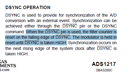
    If DSYNC is low, the modulator will stay in a reset condition and a conversion will never complete.  As I mentioned previously RESET, PWDN and DSYNC must all be high for normal operation.

    You must have a clock source or you will not have a conversion. If you are using an external clock source, the clock input is on the XIN pin.  XOUT is only used with a crystal/resonator as a force to generate oscillation.  XOUT is an output pin, which should be left floating when not used.  The external clock frequency must be 1MHz or greater, but less than or equal to 8MHz.

    Best regards,

    Bob B

  • Got it. All those crieteria are met. In the process of connecting DSYNC/ high.
  • That did it. Gathering data now. Thank you.
    I have to tell you Bob, your line "If DSYNC is low, the modulator will stay in a reset condition and a conversion will never complete" by all rights should be in the spec sheet. I could just as well envison the DSYNC/ pin being a logic OR function (not AND as it must be) with the register DSYNC bit, in which case I would need to pull it low for the register bit to control DSYNC/.
  • Hi Jim,

    I'm glad you got it working.  I understand your confusion.  I didn't write the datasheet and unfortunately there are some things that are not clear.  However there are some hints and information throughout the datasheet such as on page 14 which shows the following:

    Best regards,

    Bob B

  • Hi Jim,

    There was one other thing I forgot to mention.  There is no DSYNC bit within the registers, but rather a DRDY bit that follows the DRDY pin (which is an output).  There is the DSYNC command that will mimic the behavior of the DSYNC pin.

    Best regards,

    Bob B

  • Where does it say the modulator can't be held in reset to retrieve the data.?
    I give. You'll never aggrea that spec sheet is shining example of too sparse info.
  • How about an example schematic for instance?
  • Hi Jim,

    Actually I do agree that the information in the ADS1217 datasheet is limited and a number of things are unclear or missing.  This is something that we are trying to cover better with our newer devices.  For example, you can look at the ADS1220 datasheet as an example of the types of discussions and applications information we are now providing.  Unfortunately we do not have the resources to go back and fix up all of the older device datasheets at this time.  We are attempting to do so, but the process is slow as there are so many devices.  In the meantime please feel free to ask questions using this forum if you have any doubts. We have learned many things along the way and are still learning.  We also appreciate the comments and feedback.

    Best regards,

    Bob B

  • Thanks Bob. I imagine you sensed my frustration with that. I really appreciate your help in any case.

  • Hi Bob,

    Now that we are gathering data from the ADS1217 we are on to the next set of problems.

    Our data seems quite messed up and/or random for how we have the device configured. See the following emulator log that shows how we have the device set up according to the line starting with $4 toward the bottom. This is read of the internal registers.

    Note we have a hex 88 in the second byte which controls the input MUX. With this as such we are connecting both the plus and minus input of the DAC to analog GND. So I would expect to see relatively minor excursions just due to the noise floor.

    I have to say the spec sheet doesn't tell us explicitly what the format of the data will be. I see the M/DEC1 register alludes to it. It looks like if we have U/B(not) set to 0 it is bipolar and ,the data will be 2's compliment. Conversely if U/B(not) is set to 1 it will be unipolar and, the data will be unsigned. We have a hex 87 in the M/DEC1 register which means the format will be bipolar/ 2's compliment.

    Note the table that follows, sample buffer, which is retrieved data. There are some wildly varying values no matter if we use unsigned, 1's compliment, or 2's compliment to decode. It looks to me like the sign bit is being dropped randomly in some cases.

    1. Can you explain what the format is?

    2. Note, after reset, we never get a 67 in the last register but rather a 00 which is counter to the spec sheet. Is this a problem?

    3. I put too much capacitancae on VRCAP initially. I had a 10uf  electrolytic in parrallel with a 0.1 ceramic. I see now in the data sheet the recommendation is just 0.001uf. However, I found a schematic of a demo board on your web site with a 0.1uf. I have removed the 10uf electrolytic. Is it possible I damaged the device?

    Jim

  • oops - forgot the attachment.
    Further oops - looks like I can't attach anything.
    Please advise
  • Finally figure out you need enhance format. Here's the attachment .

    Inline image 1

  • Hi Jim,

    You need to use the rich format option to insert a file or picture.  You can only attach one file per post, so if you have multiple files I suggest zipping them first.  You can insert many pictures if required, but they have to be in a file format to upload...in other words you cannot cut and paste the graphics.

    You may have some communication issues.  Do you have any logic analyzer or scope shots of the communication?  Can you send me all of the register settings that you are using?  We need to verify that what you think you are reading and writing to the device is actually correct. First, before running any calibration routines, what values do you read from all the registers after power up?  Also, can you send my your schematic just to make sure you have everything connected properly since we don't have an example applications circuit in the datasheet?

    One issue you may be seeing is related to common-mode.  Register default is buffer enabled and you have a restriction that requires you to be at least 50mV above AGND for the input.  If you measure with respect to AGND, you need to run with the buffer off. See the Electrical Characteristics table on page 2 under Analog Input Voltage.

    The Unipolar/Bipolar data output format allows you to either measure a +/- voltage (B with sign bit), or a single-ended voltage (U with all bits available in a single measurement direction).  In either case you can measure a single-ended voltage, but in the unipolar case you recapture the sign bit increasing the dynamic range.  This may or may not be significant depending on the noise of your input signal.  In the bipolar case when measuring close to 0V, you will see noise that will result in returned values both + and -.  Remember that -1 code is 0xFFFFFF in the bipolar case.

    You should see the 0x67 in the last register unless you have either written an incorrect value or if a calibration routine changed the value.  If the value is truly 0x00, this will effect the result dramatically.

    As to having too much capacitance on the VRCAP pin, sometimes an oscillation can occur but the biggest problem will be the reference settling time after power up.  I would suggest keeping the VRCAP at 0.1uF or smaller.  This should not have damaged the device.

    Best regards,

    Bob B

  • I was able to attach a file eventually. Did You see it?
    The data is odd.
    We issued a reset before doing a conversion.
    Wouldn't this negate calibration?
    Just as a test to make sense of the data we connected both inputs, plus and minus, to AGND internal to the chip. See page 16 under MUX. If you put a 1 in the highest bit place you internall connect the inputs to AGND. I don't expect to generate absolute zero, but do expect them the value to be within 0.5% of zero I would think. We see a 2's compement number corresponding to of 50% of the range.
  • So given our register setup with buffer enabled and plus and minus connected to AGND internally, are you saying we must turn the buffer off for a valid measurement?
  • Hi Jim,

    All I see is a block x where the attachment should have been.  AINCOM is a common input.  Do you have it physically connected to AGND?  As to the buffer, the output of the buffer cannot drive all the way to AGND, so you will be measuring in a non-linear region.  With the inputs shorted, even with the buffer enabled you should be within a fairly narrow window close to zero.  It seems more likely there is an issue with the reference to have this large of an excursion.

    Do you have VREFOUT connected to REF+ and is REF- connected to AGND?

    Best regards,

    Bob B

  • Bob, I'll retype our setup and quite a few data points for illustration. Here tis.

    Register read
    0x3a, 0x88, 0x0, 0x0, 0x0, 0x0, 0x0, 0xff, 0x80, 0x87, 0x0, 0x0, 0x0, 0x24, 0x90, 0x0

    first 24bit word in our sample bufferafter doing an aquisition:
    0xffff39, 0xffff6c, 0x7ffe06, 0x7ffe52
    0x7ffeb0, 0x7ffece, 0x7ffe9a, 0xfffe52

    2's compliment of 0x7ffe9a is a huge number for example!

    About communication, the same comm routine always reads the registers correctly. That is you read what you write with exception of the last byte which is always 00.

    I hesitate to send a sechematic on a public forum. Do you have another address?

    JIm
  • Hi Jim,

    You can contact me via:

    pa_deltasigma_apps@ti.com

    Is it possible for you to read the register contents before writing/reading back?  When you write the registers do you write them as a block, and if so do you write through register 0x0F?

    Also, can you explain to me how you are reading back the data?  Are you issuing the RDATA command or running in RDATAC mode and just reading the data?  How are you determining when to read the data?  Are you polling DRDY, using an interrupt relative to the falling edge of DRDY or are you reading the M/DEC1 register bit 7?

    If you are using the RDATA command, are you waiting the minimum of 50 tosc periods (t6 of Timing Diagram on page 7) from the last edge of the last SCLK edge of the RDATA command to the next SCLK edge for the data to be read?  You must make sure that there is enough time for the command to be decoded and the output register to be updated.

    Best regards,

    Bob B

  • Ok Bob, I sent you a schematic via the e-mail address you provided. I also sent your questions to our firmware guy and will pass his answers along to you shortly.
  • Here's the firmware guy's response to me:

    Okay, good questions.

    It's possible to read the registers before writing them. That's pretty much what I do on initialization:
    when the board comes up the ADS1217 RESET* is low, on initialization of the device I bring this high, configure the SPI interface and send a RESET command. After a pause I read all the registers with a single RREG command, the result of which you see in the screenshot variable "regs[0]." Weirdly I read 0x87 for the M/DEC1 register instead of the reset value of 0x07, and I get 0x00 for the last register, FSR2, instead of the reset value of 0x67. After that I wrote the registers with our values one at a time, that is, using a separate WREG command for each register (with a delay between). After that I read back all the registers with a single RREG command again, the result of which you see in the variable "regs[1]." You can see here the register changes that we made.
    I was collecting data by first sending a DSYNC command, pausing for more than 1 us (well over 4*t(osc), which is 667 ns at t(osc) = 6 MHz), and then sending an RDATAC command. Thereafter I waited for DRDY* interrupts and simply read three bytes from SPI each time the interrupt struck on the low edge of DRDY*. I read the these three bytes using three separate 8-bit SPI transfers with no explicit delay between them (there's none specified in the datasheet), nor do I include any explicit delay between the assertion of DRDY* and the start of the SPI reads (there's just the interrupt latency), but there's no minimum time specified in the datasheet for this, either...
  • Hi Jim,

    That procedure is correct and should work ok.  Reading back the M/DEC1 register as 0x87 is correct if DRDY happens to be high when the register is read.  Bit 7 on this register is read only.  I'm a little stumped by the last register reading out as 0x00 unless the command to read it back is incorrect.  If the desire was to read 16 registers (0 to 0x0F), but if the command sent was to read 15, the extra clocks would read out zero as that was the last output state for register 0x0E bit 0.  The correct command should be 0x10 0x0F (RREG starting at register 0 - first byte - reading 16 registers as total number of registers less 1 - byte 2).  If the command sent is 0x10 0x0E, then you would see the result as given.  Make sure the command is correct.  Basically I would avoid reading and writing the registers 0x0A through 0x0F unless absolutely necessary to avoid any accidental writes.

    Another thing to try and do is issue a SELFCAL.  One other note is DSYNC does not need to be issued each measurement cycle and in fact isn't necessary at all unless you need to synchronize to some event, or if you need to restart a conversion for some reason.

    It would be helpful to see logic analyzer or scope shot data of the communication just to rule out any simple issues related to timing.  It appears that the timing is ok, but based on the values returned it would appear that you are missing the most significant bit.  You could try slowing down the SCLK a little to see if that helps.

    Best regards,

    Bob B

  • Mark's response:

    I'll try but your advice conflicts with the datasheet, though. According to the datasheet the count sent in the RREG command is supposed to be the number of registers you want less one. So if I want 16 registers I'm supposed to send a count of 0x0e, which I do. I dimly recollect trying 0x0f and getting some other failure, but much water has passed under the bridge since then, so I'll try again with our hardware mods. I can try slowing the SCLK too, but that would be a pretty lame solution as the SCLK is already at 75% of it's maximum...

    Jim here, I plan to travel to Mark's place to take a look at the communication timing tomorrow. It would be ashame ($) to throw our hands up and design the device out.
  • Hi Jim,

    Ok now some of this makes sense relative to interpretation.  Basically the number of total registers is 16 with addressing from 0 to 0x0F.  In hex, the number 16 is 0x10, so the number to start with is 0x10.  One less than 0x10 is 0x0F.  This starts to make sense when you think of reading just one register.  With the programmer's interpretation this would be impossible.  At this point I'm wondering if this same issue is occurring on the register writes in some way as the addressing is the same in both cases.

    If it would help we could set up a conference call to work through some issues.

    Best regards,

    Bob B

  • Yes, Let's set up a call.
    Are you central time?
    We are Eastern time. I plan to be at Mark's place at 10:30am et.
    Shall we call you?
    Phone number?
    reply to jimp@gpms-vt.com if you like.
  • Hi Jim,

    I tried getting ahold of you earlier today and did talk to Mark.  I told Mark I would do some investigation on any required delay following DRDY going low.  I did not find any specific information for the ADS1217, but I did find some information with respect to the ADS1241 which has a very similar digital operation.  This datasheet specifies a delay of 10 tosc delay for the time between DRDY going low to the start of SCLK.  This information is on page 6 of the ADS1241 datasheet as t19.  Please forward this information to Mark as I believe this would be the appropriate delay for the ADS1217 as well.

    Thanks,

    Bob B