This thread has been locked.

If you have a related question, please click the "Ask a related question" button in the top right corner. The newly created question will be automatically linked to this question.

JESD204B data corruption (TSW14J56EVM+ADC12J2700EVM)

Other Parts Discussed in Thread: ADC12J2700EVM, LMK04828, ADC12J2700

We are having an issue with the ADC12J2700EVM, where the data from the JESD204B test modes are corrupted at the output of the JESD204B IP interface inside the Arria V FPGA on the TSW14J56EVM board. The ramp test mode is corrupted in the same way as the forum post below:

https://e2e.ti.com/support/data_converters/high_speed_data_converters/f/68/t/466492

The above design uses a Xilinx part but seems to still suffer from the same issue as our design, which is implemented in an Altera part!

Below is a SignalTap screenshot of the corrupted data for the ramp test:


 The initial startup including CGS and ILA operates correctly as observed in the pcs_data register inside the Altera IP block.

The attached text file shows the output from the rx_dataout register of the Altera IP block.


ramp test.txt
A0A1A2BC
A4BAB9A7
A8B6B5B4
B3B2B1AF
B0AEADAC
ABAAA9B7
B8A6A5BB
A3BDBEBF
6061627C
647A7967
68767574
7372716F
706E6D6C
6B6A6977
7866657B
637D7E7F
8081829C
849A9987
88969594
9392918F
908E8D8C
8B8A8997
9886859B
839D9E9F
4041425C
445A5947
48565554
5352514F
504E4D4C
4B4A4957
5846455B
435D5E5F
2021223C
243A3927
28363534
3332312F
302E2D2C
2B2A2937
3826253B
233D3E3F
E0E1E2FC
E4FAF9E7
E8F6F5F4
F3F2F1EF
F0EEEDEC
EBEAE9F7
F8E6E5FB
E3FDFEFF
0001021C
041A1907
08161514
1312110F
100E0D0C
0B0A0917
1806051B
031D1E1F
C0C1C2DC
C4DAD9C7
C8D6D5D4
D3D2D1CF
D0CECDCC
CBCAC9D7
D8C6C5DB
C3DDDEDF

We have spent a lot of time on this problem and neither the TI or Altera engineers have been able to explain what is happening.

Is anyone able to explain what is happening and offer a solution?

  • Hi Ross

    Can you provide the details of the ADC clock frequency, clock source (internal or external), device decimation/format mode you are using?

    Are you changing any of the LMK04828 divider settings to optimize the FPGA clock frequencies for the Xilinx FPGA?
     If so, please let us know which registers are changed and what the new values are.

    Data scrambling is enabled by default in the ADC. Is scrambling enabled in the Xilinx JESD204B firmware?

    As noted on the ADC12J2700EVM schematic FMC connector page, the 8 data lanes are inverted in polarity with respect to the standard FMC pin mapping.

    Is your receive firmware compensating for the inversion?

    Is your Xilinx firmware based on the example IP provided with the TSW14J10EVM?

    Hopefully we can get you up and running soon.

    Best regards,

    Jim B

  • Hi Jim,

    Just to clarify we are using the TSW14J56EVM, which has an Altera Arria V FPGA not a Xilinx. 

    The ADC is running at 2.7GSps and the LMK04828 outputs a 135MHz clock to the FPGA across the FMC connector. We are running with no decimation in the ADC. 

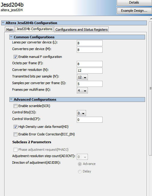
    The image shows the format of the JESD204B link and we have tried playing around with these settings but they do not seem to affect data at the link layer.

    We have not changed any LMK04828 settings from the default given by the ADC12J2700EVM GUI A software.

    We have turned off scrambling in the Altera IP and the ADC.

    We currently believe that the JESD IP from Altera automatically detects lane polarity and will adjust accordingly.

    We haven't based our design off the TSW14J56EVM example. We are only using the JESD204B IP from Altera. I did note that in your design example there is a module inside Qsys called jesd_top_qsys_0 that is your instantiation of the Altera IP but with extra files written by TI. We are not sure what these files are doing as they are un-commented, for example jesd_rx_top.v by Ebenezer Dwobeng.

    Thanks,

    Ross

  • Ross,

    The ‘jesd_top_qsys’ module has all the “JESD interface” related instantiations like xcvr Rx and Tx native PHYs, JESD Rx and Tx IPs, Reconfiguration & Reset controllers and transport layer. Please find the details of modules present under ‘jesd_top_qsys’ in the following:

    • ·         jesd_top: Instantiations for jesd_rx_top, tx_top, clk rst gen module and transceiver reconfiguration controller are done here.

    o   jesd_rx_top: Contains JESD Rx Interface related signals and instantiations

    §  jesd204b_mc_rx: JESD Base Only Rx Mega Core IP from Altera

    §  jesd_dec_xcvr: Contains XCVR native PHY and reset controller instantiations.

    §  Altera_jesd204_transport_rx_top: Performs 32bit per lane and shift registered data output operation based on number of lanes. Kindly note that, all other transport layer related operations are performed in software layer (DLL) in PC.

    o   jesd_tx_top: Similar to jesd_rx_top module, it has JESD Tx related signals and instantiations.

    o   jesd_clk_rst_gen: Contains PLL to generate Rx and Tx line rate by 40 clocks from JESD Device Reference Clock.

    o   jesd_enc_avgx_reconfig_cnrl: Transceiver Native PHY reconfiguration controller.


    Based on the ADC12J2700 schematics, we need to invert the Serial Data from ADC (i.e., We need to invert the ‘PCS output data’ from PHY). If the JESD IP is configured for both “Base and PHY”, then these setting (lane_polarity) has to be applied for the JESD IP. Otherwise, if native PHY is used then we have to set the ‘std_polinv’ signal for all the PHYs.

    Regards,

    Jim

  • Ross,

    From the ‘ramp_test.txt’ file attached by you, it looks like the issue is with respect to the ‘lane polarity’.


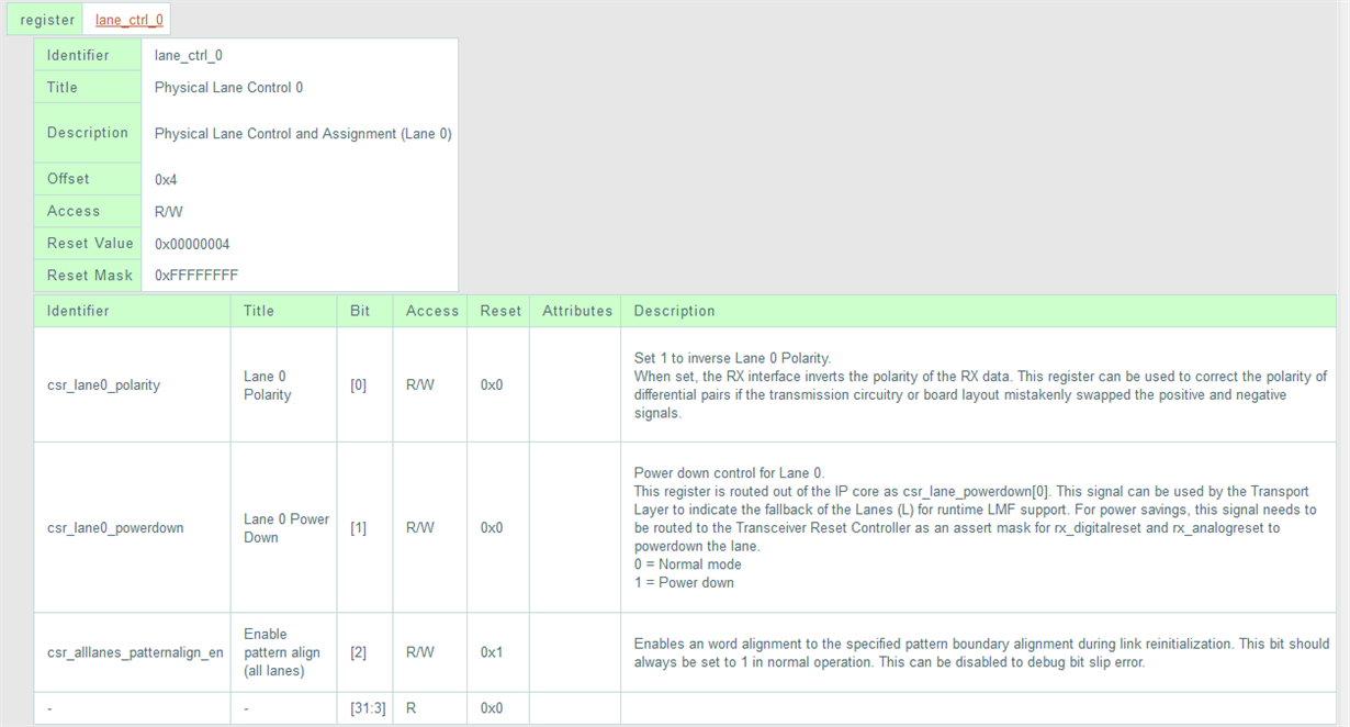
    We are assuming from the post that you are using JESD Mega Core IP for “PHY’ also. We have to perform the ‘CSR Register Write’ to the ‘lane_ctrl_0’ register of JESD IP with 0th bit set high, to inverse the lane polarity. Please find the attached screenshot from “JESD IP’s RX Register Map” regarding ‘lane 0’ polarity inversion register bit details. Also note that, we have to perform this register write for all the used physical lanes.


    Kindly note that, if ‘Base and PHY’ are configured separately, we have to connect the ‘csr_lane_polarity’ from “JESD Base IP” to “PHY IP” in addition to above register write.


    Try using ‘Long/Short Transport Test Pattern’ and observe how data is being received in the signal tap, and see if this fix helps resolve the issue.

    Regards,

    Jim

  • Hi Ross

    Were you able to make any progress with this issue?

    Best regards,

    Jim B

  • Hi,

    Thanks for your help. This has solved the issue!

    I am still confused as to why it works, as I don't understand how it did CGS and ILAS with reversed polarity lanes?

    Thanks,

    Ross

  • Hi Ross

    With inverted lanes the CGS will still work because the K characters are just inverted when the running disparity changes from +1 to -1.

    The ILAS probably shouldn't work, as D characters don't follow the same simple inversion that K characters do. I think that example IP doesn't do full ILAS verification, and that is why you are able to proceed to the normal data phase.

    Best regards,

    Jim B