


Hi,
Could you please give us your advice about the following questions ?
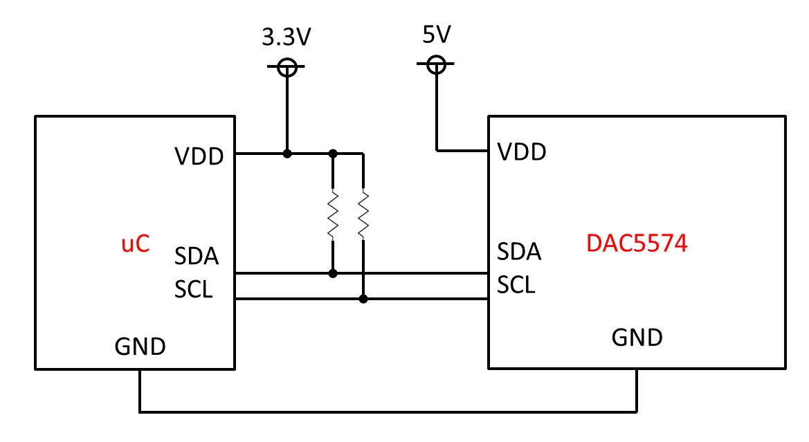
Q1. I2C Bus Connection
Is it possible to connect I2C bus as below ?
Q2. Threshold for Input Low/High Voltage for SCL SDA
Could you please tell us the threshold of the input low / high voltage for SCL and SDA if possible ?
Q3. Power-on Sequence
The 3.3V is supplied to the SCL and SDA pins for DAC5574 if the power supply(5V) for DAC5574 is turned off before the power supply(3.3) for uC is turned off.
Is it possible to apply the above power-on sequence ?
Best regards,
Kato


