This thread has been locked.

If you have a related question, please click the "Ask a related question" button in the top right corner. The newly created question will be automatically linked to this question.

LMP90100 - VHDL/Verilog interface code

Other Parts Discussed in Thread: LMP90098, LMP90100, LMP90080

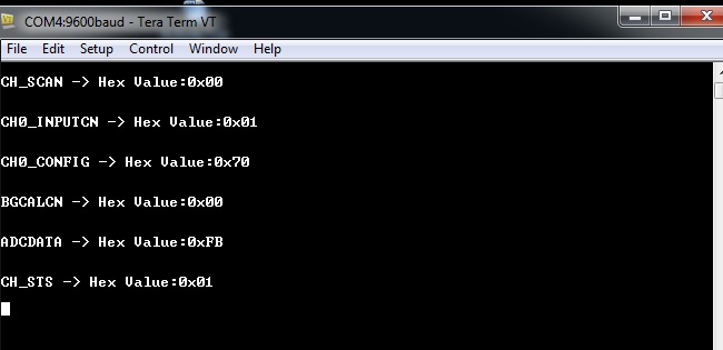
Can I get any reference VHDL/Verilog code for interfacing LMP90098 to FPGA. I do not have any microcontroller on our custom board. i tried to use SPI communication using microblaze softprocessor but could not succeed.

I tried to code myself as per the datasheet but could not succeed.

  • Hi Aditya,

    We have some C code available. Go to the the LMP90100 web page and click on the Tools and Software tab. Download the MSP430 Interface to LMP90100 Code Library. This has some examples that you can follow.

    Mike
  • sir i got the flow of logic from earlier forum replies

    i have a basic issue - the case when csb is tied low then how the transaction1 and transaction2 are descriminated.

  • Hi Aditya,

    If you have CSB tied low, you write to it in the same way.  Transactions 1 and 2 are set by the data sent.  For example, if you are going read two bytes starting at register 0x25 you would send (see Figure 67): 

    Transaction1

    00010000 00000010

    Transaction2

    10100100

    Zeros sent during data read

    00000000 00000000

    During this time CSB can be held low.  The LMP90080 recognizes transaction 1 from the data being sent. 

    If you use this method where CSB is always low, you cannot use streaming mode because you have to de-asserte CSB to get out of streaming mode. 

    You also have to be careful that you always send the correct data in the correct format and order, because if you get it mixed up the part will not know what to do with what you sent. 

    Mike

  • Hi Aditya,

    It is Figure 73 in the LMP90100 datasheet, Figure 67 in the LMP90080 datasheet.

    Mike
  • hi

    thank you for your reply

    i am able to successfully read/write registers via my VHDL code. The issue now is I am unable to read ADC_DOUT successfully. When reading i am getting some junk values --
    FF
    F4
    00
    04 etc

    my sclk freq is 750khz (approx)

    i am providing more than 72 us delay between successive reads of ADC_DOUT

    when reading CH_STS register i m getting 0x01 that means => "ADC_DOUT just read was either invalid (not ready) or there was a repeated read"

    FYI-
    i am working on
    1. ScanMode0: Single-Channel Continuous Conversion
    2. DRDYB Case1: Combining SDO/DRDYB with SDO_DRDYB_DRIVER = 0x00
    3. all registers are set to default - verified after reading back


    Kindly help with pointers !!!!
  • Hi Aditya,

    Please send me a listing of the values you have in all your registers.

    Thanks,

    Mike
  • Sir the code is written for reading one byte at a time

    I have checked the default values till address 0x1f registers. It shows all default values mentioned in data sheet.

    First non default value was read for CH_STS. WHICH meant invalid data read

    Then i added delay of 100 us after first transaction. But again i am reading some junk data at ADC DATAH. Other than this i am reading correctly
  • my code: i am unable to attach file so copying in this manner.. kindly try to read..


    library IEEE;
    use IEEE.STD_LOGIC_1164.ALL;
    use IEEE.STD_LOGIC_UNSIGNED.ALL;
    use IEEE.STD_LOGIC_ARITH.ALL;

    entity rtd_logic9 is
    Port ( gclk : in STD_LOGIC;
    sclk : out STD_LOGIC;
    csb : out STD_LOGIC;
    sdi_mosi : out STD_LOGIC;
    sdo_miso : in STD_LOGIC;
    test_data : out STD_LOGIC_VECTOR (7 downto 0));
    end rtd_logic9;

    architecture Behavioral of rtd_logic9 is

    type state_type is (S0, S1, S2, S3, S4, S5,S6,S7, S8, S9, S10, S11, S12, S13, S14, S15, S16, S17, S18, S19, S20, S21, S22, S23, S24, S25, S26, S27 ,S28, S29, S30, S31, S32, S33, S34,S35,S36,S37,S38,S39,S40,S41,S42,S43,S44,S45,S46,S47,S48,S49,S50,S51,S52,S53,S54,S55,S56,S57,S58,S59,S60,S61,S62,S63,S64,S65,S66,S67,S68,S69,S70,S71,S72,S73,S74,S75);
    signal next_state:state_type;
    signal current_state:state_type := S0;

    signal trans1: std_logic_vector(15 downto 0):= (others=>'0');
    signal trans2: std_logic_vector(15 downto 8):= (others=>'0'); -- note this is not [15..0]

    SIGNAL cnt: std_logic_vector(13 downto 0):= (others=>'0');
    SIGNAL cnt1: integer range 0 to 1024:= 0 ;
    SIGNAL cnt2: integer range 0 to 1024:= 0 ;
    SIGNAL test_data_tmp: std_logic_vector(7 downto 0):= (others=>'0');
    signal csb_tmp : std_logic := '0';
    signal sdi_mosi_tmp : std_logic := '0';
    signal sclk_tmp : std_logic := '0';
    signal sclk_tmp1 : std_logic := '0';
    signal cnt_en : std_logic := '0';

    begin

    process(gclk) -- counter for clock division
    begin
    if rising_edge(gclk) then
    cnt <= cnt + '1';
    end if;
    end process;

    sclk_tmp <= cnt(6); -- 100/128 = 781.250KHz ~ 1.28 us period

    process(sclk_tmp, cnt_en)
    begin
    if cnt_en = '0' then
    cnt2 <= 0;
    elsif rising_edge(sclk_tmp) then
    cnt2 <= cnt2 + 1;
    end if;
    end process;

    process(sclk_tmp)
    begin
    if(falling_edge(sclk_tmp)) then
    current_state <= next_state;
    end if;
    end process;

    trans1 <= "0001000000000001"; -- trans1 for reading data at 0x1A
    trans2 <= "10001110"; -- trans2 for reading data at 0x1A

    process(current_state, sdo_miso, sclk_tmp, trans1, trans2, cnt2)
    begin

    case current_state is
    when S0 =>
    csb_tmp <= '1';
    sclk_tmp1 <= '1';
    sdi_mosi_tmp <= '0';
    next_state <= S1;
    cnt_en <= '0';
    when S1 =>
    csb_tmp <= '0';
    sclk_tmp1 <= '1';
    sdi_mosi_tmp <= '0';
    if falling_edge(sdo_miso) then
    next_state <= S2;
    else
    next_state <= S1;
    end if;
    when S2 =>
    csb_tmp <= '0';
    sclk_tmp1 <= sclk_tmp;
    sdi_mosi_tmp <= trans1(15);
    next_state <= S3;
    when S3 =>
    csb_tmp <= '0';
    sclk_tmp1 <= sclk_tmp;
    sdi_mosi_tmp <= trans1(14);
    next_state <= S4;
    when S4 =>
    csb_tmp <= '0';
    sclk_tmp1 <= sclk_tmp;
    sdi_mosi_tmp <= trans1(13);
    next_state <= S5;
    when S5 =>
    csb_tmp <= '0';
    sclk_tmp1 <= sclk_tmp;
    sdi_mosi_tmp <= trans1(12);
    next_state <= S6;
    when S6 =>
    csb_tmp <= '0';
    sclk_tmp1 <= sclk_tmp;
    sdi_mosi_tmp <= trans1(11);
    next_state <= S7;
    when S7 =>
    csb_tmp <= '0';
    sclk_tmp1 <= sclk_tmp;
    sdi_mosi_tmp <= trans1(10);
    next_state <= S8;
    when S8 =>
    csb_tmp <= '0';
    sclk_tmp1 <= sclk_tmp;
    sdi_mosi_tmp <= trans1(9);
    next_state <= S9;
    when S9 =>
    csb_tmp <= '0';
    sclk_tmp1 <= sclk_tmp;
    sdi_mosi_tmp <= trans1(8);
    next_state <= S10;
    when S10 =>
    csb_tmp <= '0';
    sclk_tmp1 <= sclk_tmp;
    sdi_mosi_tmp <= trans1(7);
    next_state <= S11;
    when S11 =>
    csb_tmp <= '0';
    sclk_tmp1 <= sclk_tmp;
    sdi_mosi_tmp <= trans1(6);
    next_state <= S12;
    when S12 =>
    csb_tmp <= '0';
    sclk_tmp1 <= sclk_tmp;
    sdi_mosi_tmp <= trans1(5);
    next_state <= S13;
    when S13 =>
    csb_tmp <= '0';
    sclk_tmp1 <= sclk_tmp;
    sdi_mosi_tmp <= trans1(4);
    next_state <= S14;
    when S14 =>
    csb_tmp <= '0';
    sclk_tmp1 <= sclk_tmp;
    sdi_mosi_tmp <= trans1(3);
    next_state <= S15;
    when S15 =>
    csb_tmp <= '0';
    sclk_tmp1 <= sclk_tmp;
    sdi_mosi_tmp <= trans1(2);
    next_state <= S16;
    when S16 =>
    csb_tmp <= '0';
    sclk_tmp1 <= sclk_tmp;
    sdi_mosi_tmp <= trans1(1);
    next_state <= S17;
    when S17 =>
    csb_tmp <= '0';
    sclk_tmp1 <= sclk_tmp;
    sdi_mosi_tmp <= trans1(0);
    next_state <= S18;
    when S18 =>
    csb_tmp <= '0';
    sclk_tmp1 <= '1';
    sdi_mosi_tmp <= '0';
    next_state <= S19;
    when S19 =>
    csb_tmp <= '1';
    sclk_tmp1 <= '1';
    sdi_mosi_tmp <= '0';
    next_state <= S20;
    when S20 =>
    csb_tmp <= '0';
    sclk_tmp1 <= '1';
    sdi_mosi_tmp <= '0';
    next_state <= S21;
    when S21 =>
    csb_tmp <= '0';
    sclk_tmp1 <= sclk_tmp;
    sdi_mosi_tmp <= trans2(15);
    next_state <= S22;

    when S22 =>
    csb_tmp <= '0';
    sclk_tmp1 <= sclk_tmp;
    sdi_mosi_tmp <= trans2(14);
    next_state <= S23;
    when S23 =>
    csb_tmp <= '0';
    sclk_tmp1 <= sclk_tmp;
    sdi_mosi_tmp <= trans2(13);
    next_state <= S24;

    when S24 =>
    csb_tmp <= '0';
    sclk_tmp1 <= sclk_tmp;
    sdi_mosi_tmp <= trans2(12);
    next_state <= S25;
    when S25 =>
    csb_tmp <= '0';
    sclk_tmp1 <= sclk_tmp;
    sdi_mosi_tmp <= trans2(11);
    next_state <= S26;

    when S26 =>
    csb_tmp <= '0';
    sclk_tmp1 <= sclk_tmp;
    sdi_mosi_tmp <= trans2(10);
    next_state <= S27;
    when S27 =>
    csb_tmp <= '0';
    sclk_tmp1 <= sclk_tmp;
    sdi_mosi_tmp <= trans2(9);
    next_state <= S28;

    when S28 =>
    csb_tmp <= '0';
    sclk_tmp1 <= sclk_tmp;
    sdi_mosi_tmp <= trans2(8);
    next_state <= S29;
    when S29 =>
    csb_tmp <= '0';
    sclk_tmp1 <= sclk_tmp;
    sdi_mosi_tmp <= '0';
    next_state <= S30;
    if rising_edge(sclk_tmp) then
    test_data_tmp(7)<= sdo_miso;
    end if;
    when S30 =>
    csb_tmp <= '0';
    sclk_tmp1 <= sclk_tmp;
    sdi_mosi_tmp <= '0';
    next_state <= S31;
    if rising_edge(sclk_tmp) then
    test_data_tmp(6)<= sdo_miso;
    end if;
    when S31 =>
    csb_tmp <= '0';
    sclk_tmp1 <= sclk_tmp;
    sdi_mosi_tmp <= '0';
    next_state <= S32;
    if rising_edge(sclk_tmp) then
    test_data_tmp(5)<= sdo_miso;
    end if;
    when S32 =>
    csb_tmp <= '0';
    sclk_tmp1 <= sclk_tmp;
    sdi_mosi_tmp <= '0';
    next_state <= S33;
    if rising_edge(sclk_tmp) then
    test_data_tmp(4)<= sdo_miso;
    end if;
    when S33 =>
    csb_tmp <= '0';
    sclk_tmp1 <= sclk_tmp;
    sdi_mosi_tmp <= '0';
    next_state <= S34;
    if rising_edge(sclk_tmp) then
    test_data_tmp(3)<= sdo_miso;
    end if;
    when S34 =>
    csb_tmp <= '0';
    sclk_tmp1 <= sclk_tmp;
    sdi_mosi_tmp <= '0';
    next_state <= S35;
    if rising_edge(sclk_tmp) then
    test_data_tmp(2)<= sdo_miso;
    end if;
    when S35 =>
    csb_tmp <= '0';
    sclk_tmp1 <= sclk_tmp;
    sdi_mosi_tmp <= '0';
    next_state <= S36;
    if rising_edge(sclk_tmp) then
    test_data_tmp(1)<= sdo_miso;
    end if;
    when S36 =>
    csb_tmp <= '0';
    sclk_tmp1 <= sclk_tmp;
    sdi_mosi_tmp <= '0';
    next_state <= S37;
    if rising_edge(sclk_tmp) then
    test_data_tmp(0)<= sdo_miso;
    end if;
    cnt_en<= '0';
    when S37 =>
    csb_tmp <= '0';
    sclk_tmp1 <= '1';
    sdi_mosi_tmp <= '0';
    if rising_edge(sclk_tmp) then
    test_data <= test_data_tmp;
    end if;
    next_state <= S38;
    cnt_en <= '1';
    when S38 =>
    csb_tmp <= '0';
    sclk_tmp1 <= '1';
    sdi_mosi_tmp <= '0';
    --cnt_en <= '1';
    if cnt2 > 100 then
    next_state <= S0;
    else
    next_state <= S38;
    end if;
    when others =>
    next_state <= S0;
    end case;

    end process;

    csb <= csb_tmp;
    sclk <= sclk_tmp1;
    sdi_mosi <= sdi_mosi_tmp;

    end Behavioral;

  • sir i have got one more doubt

    while reading data - why the Transaction1[15..8] should be 0x10 -- i.e during URA setup INST1 byte is 0x10 instead of 0x90

    -- as per the description given it should be 0x90 but according to example given in data sheet its 0x10. AND moreover the logic works only when we put INST1=0x10 while reading

    under what case the INST1 should be 0x90 ????

    kindly reply at the earliest
  • Hi Aditya,

    When reading data the transaction 1 uses a write command to set the URA. The read command comes in the first bit of transaction 2.

    I am not aware of a time when the command 0x90 would be used. This first byte is always used to set the URA and so it will always be writing the address.

    I was not able to see the actual settings of the registers in the code you pasted. I will need a listing of the values of the registers to help further.

    Mike
  •  sir plz find attached screenshot of the UART output

    my vhdl logic reads the registers and register content is read back by a soft microblaze processor and displayed using UART port

    i hope this is the listing u were mentioning about

  •  sir plz find attached image

  • Hi Aditya,

    Your code shows you are setting it up for one channel, CH0, using VIN0 and VIN1. Gain is set to 1x and you are using VREF1. Background calc is off.

    How do you have the clock register, 0x12, set? Internal or external depending on what clock you are using.

    What are the voltages on the VREFP1 and VREFN1 pins?

    What are the voltages on the IN0 and IN1 pins?

    When you read the ADCDATA it shows only one byte. What are the values of the other two bytes?

    Mike