This thread has been locked.

If you have a related question, please click the "Ask a related question" button in the top right corner. The newly created question will be automatically linked to this question.

Unable to read data from ADS1293 using CC2541 (wireless heart rate monitor reference design)

Other Parts Discussed in Thread: CC2541, ADS1293, TIDA-00096

Hello

I am trying to communicate between ADS1293 and CC2541. I got my PCBs made based on the Wireless Heart Rate Monitor reference design (link: http://www.ti.com/tool/TIDA-00096). I also got the firmware from here.

I did not observe any notification data when ECG notification was enabled (using BTool).

When I observed the SPI signals with an oscilloscope, during a write/read from ADS1293 registers I observe the following:

1. sclk consists of two bursts of 8 clock cycles each, as opposed to a continuous burst of 16 cycles, which is the requirement as per ADS1293 user guide (ADS1293 EVM also shows 16 clock cycles). Is this a problem?

2. MISO line is always low (it is high in ADS1293 EVM when idle), which means that there is no data coming from ADS1293.

3. MOSI is fine - data is written MSB first, on the raising edge.

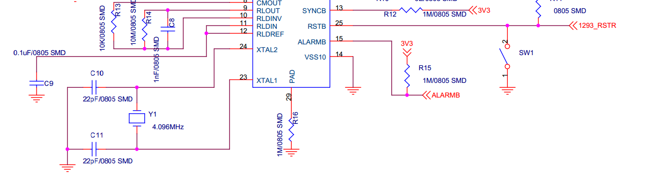
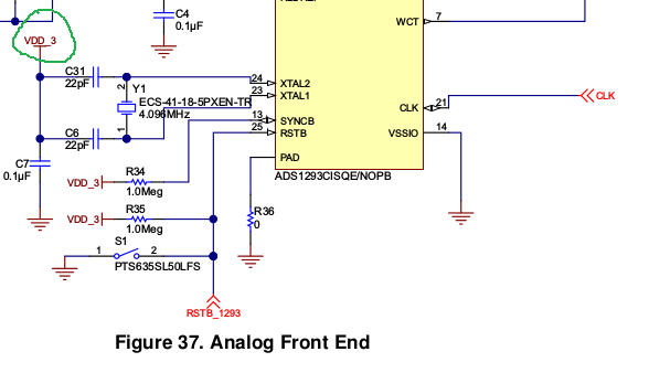
When I compared my PCB schematics with TI Reference schematics, I see that the resistor on the SDO pin is missing in my schematics. Is this a problem?

Thank you for your help.

  • Hello Sudheer,

    1. As long as CSB stays low between the two bursts it is ok. I f CSB goes high then it will think the communication is done.
    2. That is correct, that means no data from the ADS1293.
    3. Correct.
    Not having the 51 ohm resistor is ok.

    Check that your registers are set correctly as shown in the datasheet for the application. TheADS1293 will not transmit data if the registers are incorrectly set up.

    Mike
  • Hello Mike,

    Thank you for the prompt reply.

    I will check the register settings as suggested by you.

    But how do I know that settings are written into the registers. If the MOSI line shows data, is it conclusive evidence that data is being written into the registers correctly.

    I found another difference between my PCB schematics and TI reference schematics. It must be an oversight.

    My Schematic

    TI Reference

    My crystal oscillator is not connected to Vdd. Does this mean that it is not running?

    If that is the case, would SPI be affected - because SPI runs on the clock derived from SPI Master, it must be independent of the crystal oscillator.

    Thank you 

  • Hi Sudheer,

    If you have the SPI signals at the pin of the part (not probed somewhere along the trace to the part, but actually probed at the pin) the signals should be read by the ADS1293, if everything else is connected correctly.

    Yes, you need the connection of Vdd to XTAL2 and XTAL1. If the internal oscillator is not running that would make it so the SPI data does not get into the Digital Control section. The ADS1293 also will not run internally, because it does not have its clock to make it run.

    Mike
  • Thank you Mike. That answers my question.
  • Hello Mike,

    After my last conversation with you, I ran some tests with ADS EVM, and got some unexpected results. Can you please clarify.

    1. STRTCLK bit of OSC_CN register set LOW.

      This disables the clock to digital circuitry. I assume this would be equivalent of disconnecting the crystal oscillator altogether from the circuit (Am I right?)

       OUTCOME: I am still able to read and write register values through SPI (I have also checked with oscilloscope). You said previously that SPI would not                                         function without clock.

                              However as expected, the ADC does not function, and I do not see the regular blips on the DRDYB line.

    2. STRTCLK bit of OSC_CN register set HIGH

        SHDN_OSC bit set HIGH.

        409 kHz external clock given at CLK pin.

        ADS1293 must now be driven by the external clock.

        OUTCOME: As expected, I can read and write register values through SPI.

                              ADC also works well; I can see the periodic blips on DRDYB pin.

    So, I infer that reading and writing values into registers through SPI does not require the internal oscillator - the master's SPI clock is sufficient.

    The internal oscillator is only for the ADC - sigma-delta modulator and decimation filters.

    If these inferences are right, then I must be able to read and write register values with my board inspite of my crystal oscillator not being powered. But I am not - SDO remains in high impedance state always.

    Can you tell me what other problems could cause SPI not to function? I have checked that 3V3 is reaching the board correctly.

    I am troubling you because I must get a new PCB fabricated and therefore must identify all the sources of error in my board.

    Thank you.

  • Hello Sudheer,

    What you describe is following Table 6 in the datasheet.  In case 1, STRTCLK is set to 0 so no clock is going to the digital circuitry.  In case 2 you have set STRTCLK to 1 so a clock can go to the digital circuitry.  Since you are using a 409kHz clock did you also set SHDN_OSC to 1?  I think your conclusions in case 2 are correct. 

    As a final check that you can do to make sure that your SPI signals are getting into the part is to monitor IN4 and program the SELRLD bits.  Set the right leg drive to IN4 and then set it to IN6.  Do you see the voltage on IN4 changing?

    Is the SDO pin connected to something that is pulling it down?  You could try cutting the trace to that pin and see if it acts normal when not connected to the following circuitry. 

    Could the part have become damaged in testing?  The only way to make sure of this is to replace the part. 

    There is nothing that disables the SPI.  As long as you have the schematic as shown in Figure 84 and issue the commands shown in 9.2.1.2 you should see data come out of SDO.

    Mike

  • Hello Mike,

    I did not set SHDN_OSC to 1 in the first case.

    I did the check suggested by you.
    On the evaluation board, voltage on IN4 changes from 1.9mV to 3.2V when I change RLD from IN4 to IN6.
    However this does not happen in my board - neither 1.9mV or 3.2V. The pin seems to be floating (default setting of RLD).

    No, nothing is pulling SDO down.

    I have also tried with a new board (I got five of them made) and obtained the same result. Hence it is not part problem.

    My PCB design is same as wireless heart rate monitor reference design (TIDA-00096).

    The only major flaw in the circuit is that crystal oscillator is not connected to VDD.
    I guess, I can now assume that this is the reason why SPI is not working?
    Can I go ahead and get new PCBs made with this corrected?

    Thank you
  • Hello Sudheer,

    You say:
    >>On the evaluation board, voltage on IN4 changes from 1.9mV to 3.2V when I change RLD from IN4 to IN6.
    >>However this does not happen in my board - neither 1.9mV or 3.2V. The pin seems to be floating (default setting of RLD).

    This would seem to indicate that the SPI signals are not being read by the ADS1293.

    You can try reworking your current board so that the crystal is connected correctly, before you make new boards. You should probably also carefully check the rest of your board for any other differences before making more boards.

    Mike