This thread has been locked.

If you have a related question, please click the "Ask a related question" button in the top right corner. The newly created question will be automatically linked to this question.

DAC with current output (10uA to 1mA)

Other Parts Discussed in Thread: DAC9881, DAC8750, TIPD101, TIPD102

Hi Everyone,

I am looking for a DAC with current output.  The current range i am looking for is from 10uA to 1mA.

I found some TI parts that can generate from 0 to 20mA.

Is there anything i can do to the chip to convert to the desired range?

Also, I have a DAC9881 on the board, I could potentially used this generate to generate a range of voltage, however i just need to convert this into current.

Is there something i can use to convert the DAC output to current,(For my range)

Thanks a lot.

Eddy

  • Eddy,

    We might be able to come up with some circuit that would help you convert the 0-20mA output into the range that you are looking for but I don't think it would really be the most efficient solution in terms of board area and cost nor the most accurate solution. Instead I would suggest that we use the discrete approach of converting the voltage output of a discrete DAC into a current.

    There are multiple approaches to this which depend on your requirements. As a start I would suggest you look at TIPD101 and TIPD102 reference designs which illustrate low-side and high-side voltage to current converter structures, respectively.

    Please let me know if you have any further questions.

  • Kevin,

    Thanks a lot for the reply. I found your solution to be ideal for my application.

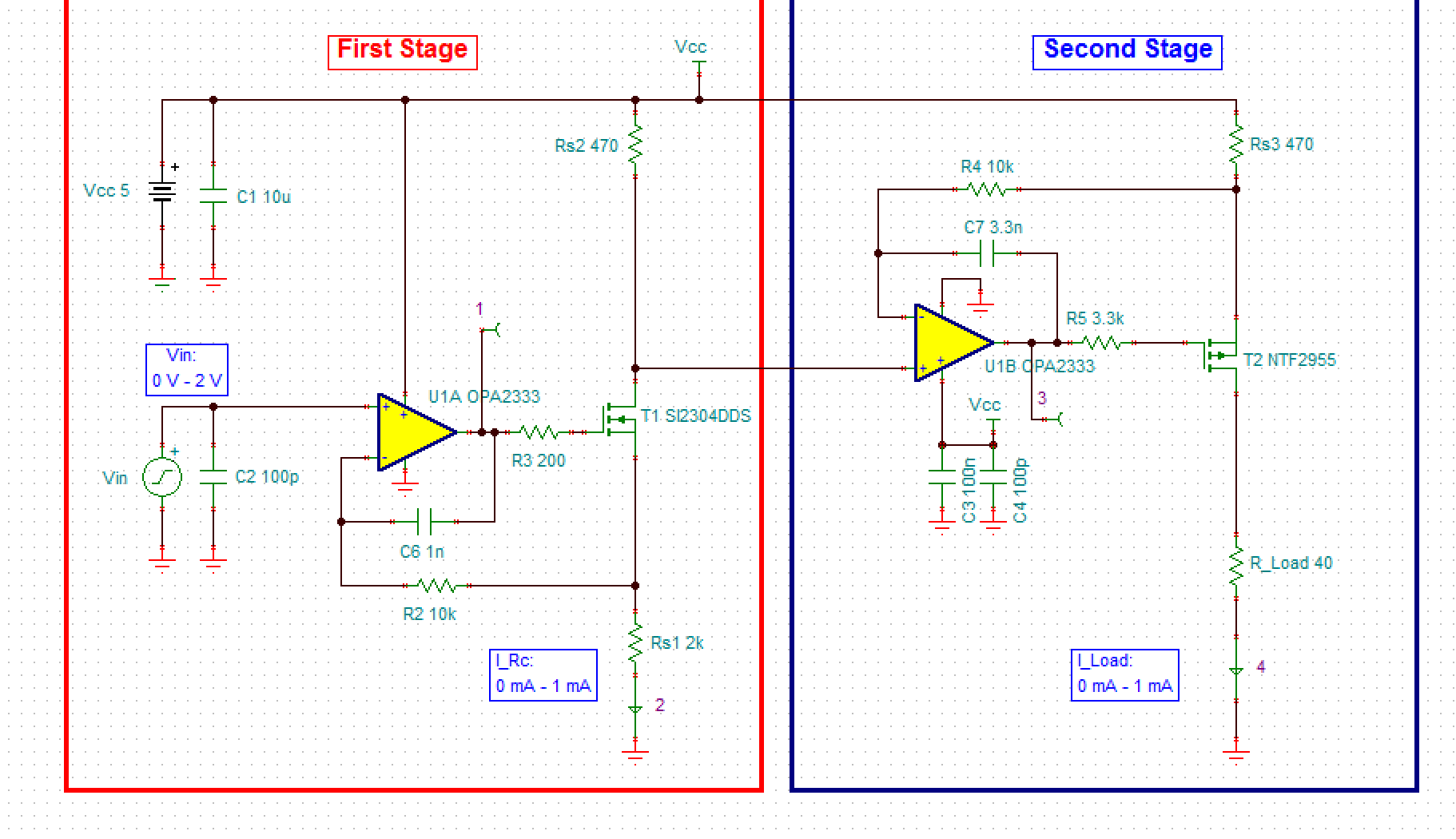
    I modified the simulation circuit( Gain setting Rs3 = 4.7 Ohm to 470 Ohm) and followed the reference document in adjusting the stability network.(R5,C7).

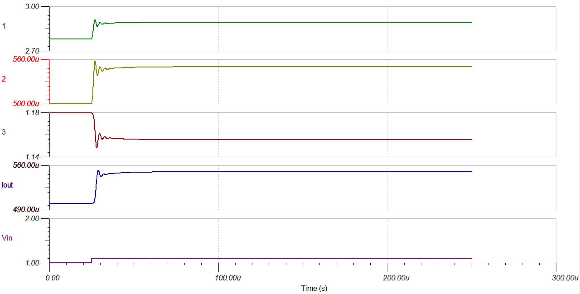
    The AC response looks stable and the output looks accurate.
    Do you mind checking this circuit see if there is anything i can improve on the circuit?

    Also 2 questions:

    1) Is there a example board for sale?  (  Since my circuit is very similar to the circuit from the tested example circuit. I would like to do a quick prototyping)

    2) What kind of load can this circuit drive?

    My understanding is that as long as the PMOS remains in Active region, The circuit will work and current output should be accurate.

    I am designing the circuit to bias transistors. (Current mirror). Will this circuit work?

    Thanks,

    Eddy

  • Eddy,

    It seems like you have done a good job following the reference design, I do not see anything that needs to be modified at this point.

    Generally speaking we do not keep PCBs on hand of these TI Designs and do not stock them for purchase, that is the case for this particular design as well, so unfortunately we cannot ship one of these designs to you for prototyping.

    Your comments about the maximum load are correct. Usually this headroom requirement for the voltage drop across the resistor and the requirements to keep the output FET in the linear region of operation is referred to as "Compliance Voltage".
  • Kevin,

    Thanks for your help,

    Regarding the MOSFET selection for NMOS, It was suggested to have a low threshold voltage.  However the BOM and SIM file has a NMOS with 2.0V threshold.

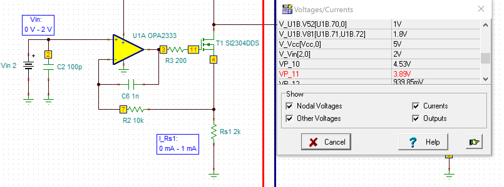
    I double checked the sim, The voltage cross the NMOS gate and source is 1.89 which is smaller than the threshold voltage. This means that the NMOP  at first stage will be off if the suggested NMOSE is used.

    I am confused, Does the Sim use the real component SPICE model?  if so why would the sim still work?

    Thanks a lot for your help,

    Eddy

  • Hi Eddy,

    The MOSFET devices in this design are inside the feedback loop of the op amps that control them.  Therefore, the op amps will use negative feedback to control the MOS Vgs voltage to achieve the desired current through the sense resistor.  The low-level currents of 0-1mA that flow through the NMOS device requires a very small VGS voltage to achieve.  Driving the FET with a voltage well above the threshold voltage would force the FET to a low-impedance state which would allow too much current to flow through it.

  • Hi Kevin and Collin,

    We got the circuit tested out today, It works great!

    Thanks a lot for your helps,

    Eddy
  • Eddy,

    Great! Let us know if you need anything else...
  • Hi Collin,

    A follow up question on the Voltage to current convertor.

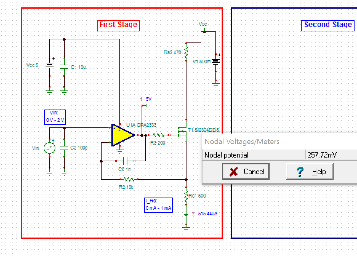
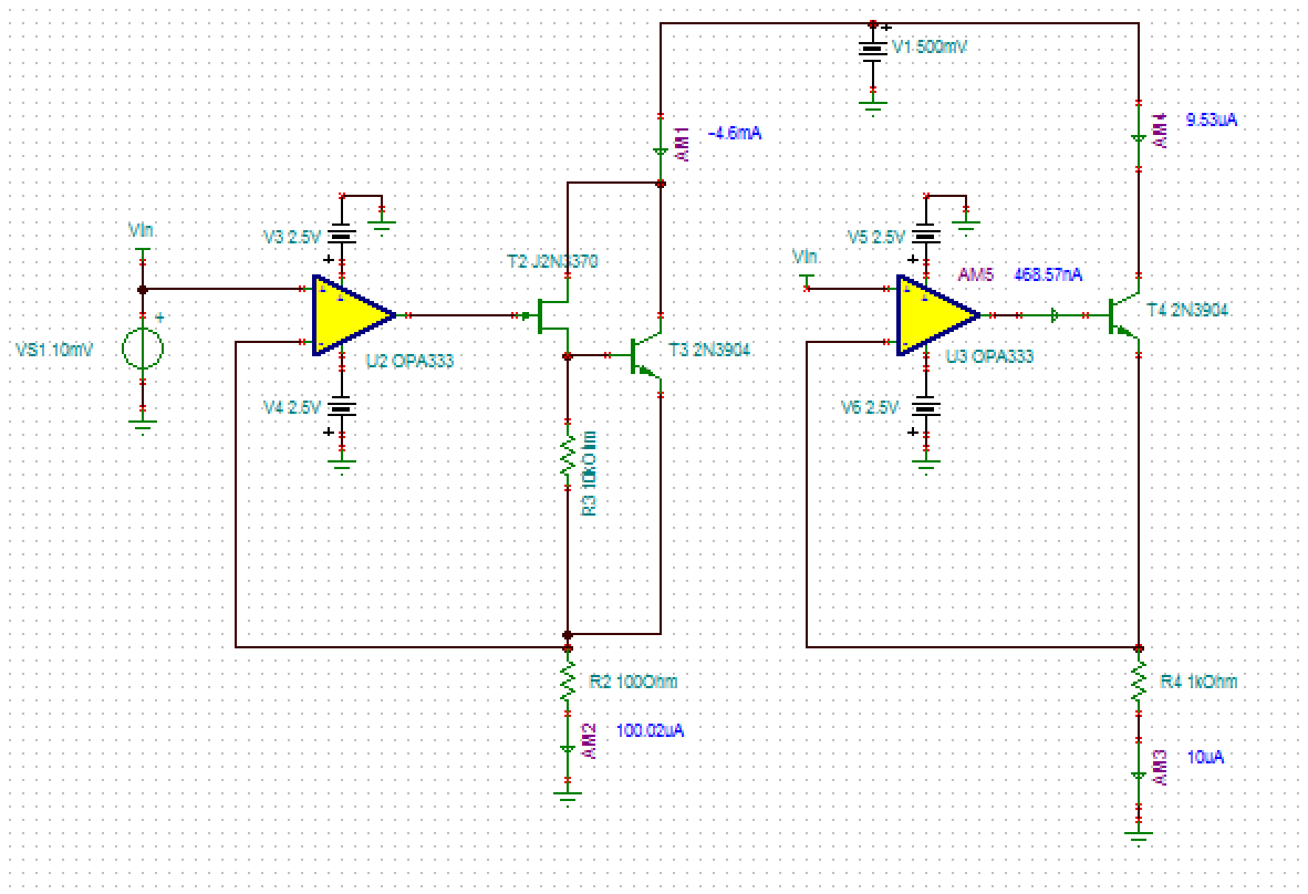
    We are trying to generate a current sink with the same range.(1uA to 1mA). I did some modification to the above circuit based on the learning from one of your past thread.().

    However, The problem i am facing is that The sink input(Vcc) have a very low voltage (~200mV), This low voltage at drain shut off the current through the transistor(Vd = Vs), therefore i am getting the current pushing through the Rs1 is no longer accurate.

    Is there any modification i can do here to make it work for low voltage at Vcc. 200mV? 

    Thanks a lot for your help,

    Eddy

    [Modification using the above circuit ]

    [Modification from the circuit in your past thread]