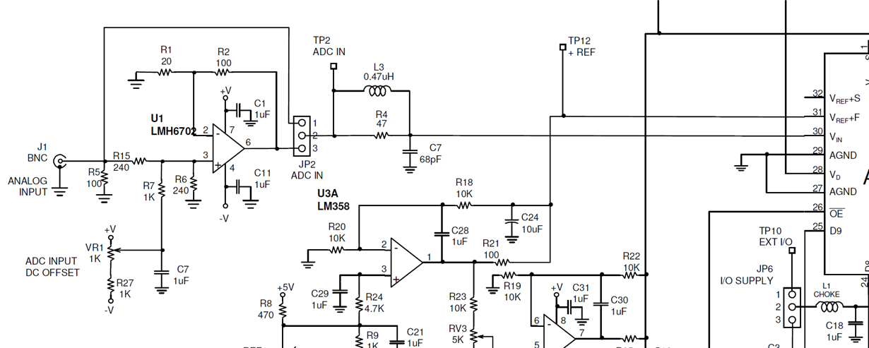
I'm using ADC10321 in my design. The sample frequency is 20MHz. The bandwidth of input analog signal is more than 100MHz. There's 20MHz noise in the capture data when input signal Vpp is 700mV. When input signal Vpp is less than 200mV, the 20MHz noise is not significant.
facts of circuits:
1. the serials resistors between the ADC digital data bus and FPGA are 110 ohms, which are put close to ADC10321.
2. the amplifier before ADC10321 is OPA698. Analog input signal is DC-coupled to ADC.
3. 6-layers PCB layout, one-point joint connection between digital and analog ground underneath the ADC device, following the layout recommendation in ADC10321 datasheet.
Is there secret of the sample and hold circuit inside ADC10321? Is there any demo board of ADC10321? Nicholas Gray's article "maintaining signal integrity enhances ADC circuit performance" (see the following web link), discussed about this issue. According to the article, it needs 100ohms and 80pf low pass filter between the amplifier and ADC input. But this kind of low pass filter can't apply to my design, because the interested signal is more than 100MHz.


