This thread has been locked.

If you have a related question, please click the "Ask a related question" button in the top right corner. The newly created question will be automatically linked to this question.

DAC3151EVM: DACCLKP/N AC coupling and simulation

Part Number: DAC3151EVM

Hi,

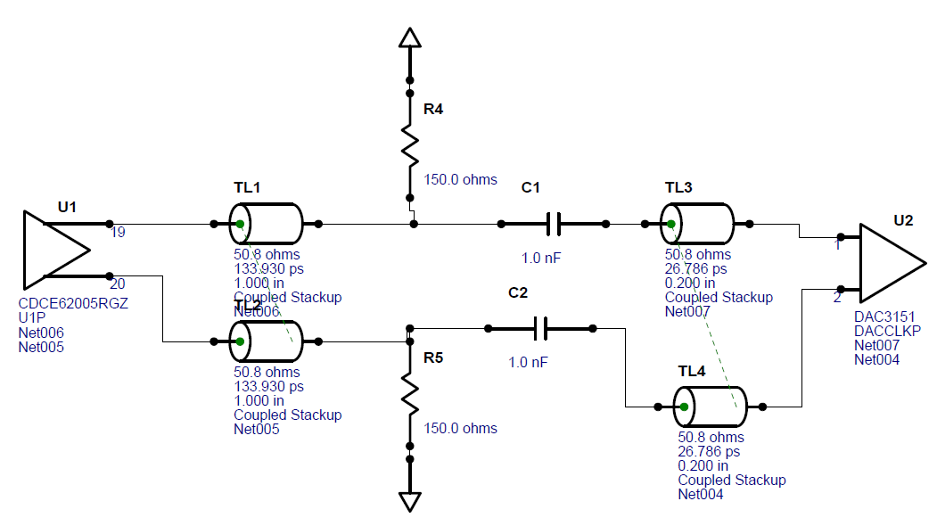
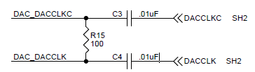
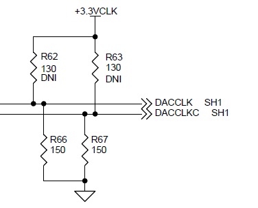
I saw this termination in evaluation module of DAC3151 at the receiver end

and the following termination at transmitter end at CDCE62005

I had the following doubts:

1) Why is the 100 ohm termination given at DAC3151 side?

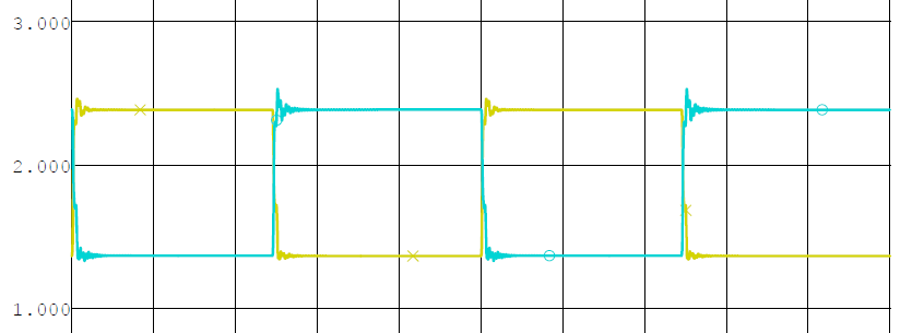
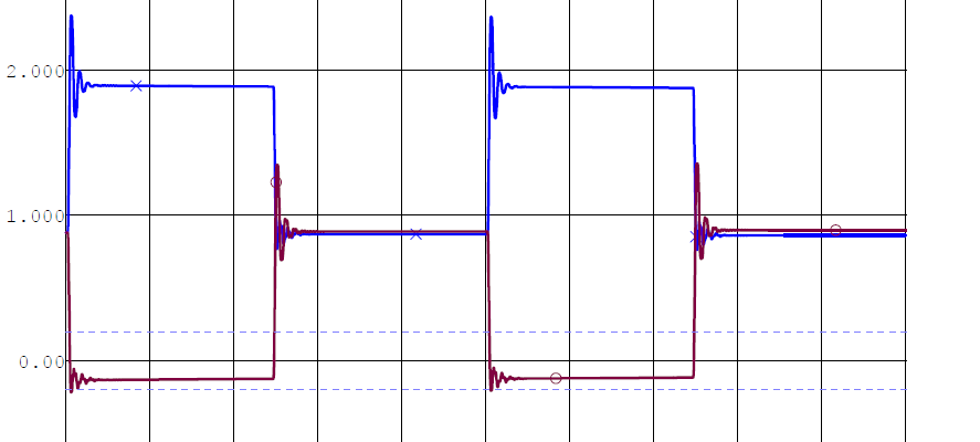
2) The interface is ac coupled so at DAC3151 there is a bias voltage of 1.8V. But I inserted the ibis model in hyperlynx and checked the voltage at the input pin it was showing dc 0.8V. Is there anything that I have to do to change to internal reference?

Regards,

Bhavya

  • Hi,

    1) An LVPECL driver is normally terminated with 50 ohms to a termination voltage of supply - 2V, or about 1.3V if the supply is 3.3V.   Sometimes instead of having to create an extra voltage for the termination, a resistive divider network is chosen such as 130 ohms to supply over 82 ohms to ground, such that the parallel combination of 130 and 82 is 50 ohms, and the 130 over 82 voltage divider yields 1.3V.   These resistors are in the schematic but not used for that.  If a PECL output is to be AC coupled, then the PECL driver needs a resistive pull down to pull the falling edge of the signal, and the resistive divider mentioned above could perform this function.  But it is easier and acceptable to just use a larger value resistor to ground, such as the 150 to ground shown in the schematic.  The size of the pulldown is usually chosen to make the slope of the falling edge match that of the rising edge and is often in the range of 120 ohms to 220 ohms.  In this case, 150 ohms.    Then after the AC coupling, the controlled impedance trace still needs a proper termination, and since the 100 ohm termination resistor is *not* included on the silicon in the DAC3151, then it is placed external to the DAC and very close to the inputs.

    2)  The clock input when AC coupled is normally about 0.9V.    When the datasheet was last updated, the editor misread the statement and turned 'LVPECL clock input for DAC core with a self-bias of approximately CLKVDD18 / 2.' into 'LVPECL clock input for DAC core with a self-bias of approximately CLKVDD18 and CLKVDD2' thinking that by CLKVDD18 / 2 meant that there was a CLKVDD18 and a CLKVDD2 rather than CLKVDD18 divided by two.    The editing error was not noticed until the datasheet was on the web. 

    '.

  • Hi,

    I have done simulation for DAC3151 ,DAC clock inputs fromCDCE62005 using hyperlynx. The circuit is as shown below:

    The input signal from CDCE62005 is shown below: I think its correct as per datasheet.

    but when the signal reaches DAC3151, the clock signals are not having a zero cross over. Is it because the big difference in common mode voltage of the two ICs?

    If so, what should I do to solve this?

    Regards,

    Bhavya

  • Sorry, the signal is not having a proper cross over not zero cross over
  • Hi Bhavya

    Your simulation schematic is missing two important details.

    1. There needs to be a 100 ohm termination resistor between terminals 1 and 2 of the DAC CLK inputs. This resistor is added at board level very close to the CLK inputs.
    2. The DAC CLK inputs are self biased to CLKVDD18/2. You can model this by adding large value resistors from a 0.9V source to terminal 1 and terminal 2. I recommend something like 100k ohms. 

    Once those are added the input voltages at terminal 1 and 2 should be correct.

    Best regards,

    Jim B

  • Hi Jim,

    I did the changes as you told me.
    But still there is no change in the signal. There is no cross over for the differential signals after ac coupling capacitor.

    Regards,
    Bhavya
  • Hi,

    I checked the ibis model to see that the DACCLK inputs are indeed modeled, as I have seen on some older ibis models that the clocking was not included in the model - but on this model the DACCLK does have a model section in the ibis file.  I know the group that created the model, so I can say that the ibis model was created from measurements on silicon, rather than simulation results as is sometimes done, so if we are still having trouble with the model after the holidays then I will ask the creator of the model to take a look at it.

    in the meantime, my suggestion would have been the same as what Jim said.   The 100 ohm termination needed to be added to the model at the DACCLK input pins as this termination is not integrated in silicon, but I wouldn't have expected the lack of differential termination to affect biasing.   Then I would have suggested adding the biasing to mid-supply just as Jim suggested, in case that aspect of the input wasn't covered in the model.  But rather than a weak biasing to 0.9V, I would have suggested a 2Kohm bias to 0.9V on each side of the DACCLK.   That is what the DACCLK input uses on the chip.  The DACCLK input is the same as used in the DAC3283, and the datasheet for that device has an equivalent input circuit in figure44 of that datasheet.   Finally, if still having trouble I would remove the DAC from your simulation completely and simply run the simulation into a 100 ohm termination with the 2Kohm biasing to 0.9V.   if *that* doesn't show the right levels, then it wouldn't be the ibis model for the DAC3151.  One thing I have seen with Spice models in the past when the biasing appears to be off is that the simulation has to run for many cycles for the biasing to 'pull' the signals to the eventual right levels if the initial conditions after the AC coupling is not close to the final conditions.  I haven't seen this issue with ibis simulations though, but I have with Spice sims.

    Regards,

    Richard P.