Because of the Thanksgiving holiday in the U.S., TI E2E™ design support forum responses may be delayed from November 25 through December 2. Thank you for your patience.

This thread has been locked.

If you have a related question, please click the "Ask a related question" button in the top right corner. The newly created question will be automatically linked to this question.

DAC3162EVM: DAC3162 EVM output FPGA Clk (LVPECL) compatibility with Xilinx AC701 Board.

Part Number: DAC3162EVM
Other Parts Discussed in Thread: CDCP1803, SN65LVDS100, DAC3162

Dear All,

I have the DAC3162EVM and the Xilinx AC701 (Xilinx Artix7 FPGA Eval Board).

The FMC connector on the DAC3162EVM and the AC701 are perfectly compatible. So I don't have any problems in connecting the two boards.

The DAC EVM Board has a TI device CDCP1803 on it. The CDCP1803 takes an external clock signal and provides the DAC Clk, FPGA Clk etc. I am able to give a 200 MHz external clock to the J9 connector of the DAC EVM and also able to tap and see the DAC Clk and FPGA Clk on the Oscilloscope. So far so good.

On the FMC connector of the DAC3162EVM, the FPGA Clk (From the DAC3162EVM board) is LVPECL standard. I have measured the  voltages of this clock and found them to be as per the datasheet of the component CDCP1803 (The swing is from 1.5V to 2.5 V for either Clk_P or the Clk_N signals). This FPGA Clk will be the input clk to the FPGA and the DAC Data will be output w.r.t. this Clk. The FPGA Clk and the DAC Clk are set at same rate.

Now, whereas the Xilinx Artix7 FPGA doesn't support the LVPECL standard and the newer Xilinx FPGAs too don't support the LVPECL standard, I want to know which other standard can I select in my FPGA so that it can still take the FPGA Clk (LVPECL) to the Xilinx AC701 Board.

The DAC3162EVM Board has mapped/connected the FPGA Clk to the D19 and C19 pins of the Artix7 FPGA.

Waiting for your suggestion.

  • Jayant,

    To me this appears to be a question for Xilinx. Is there something you need to know about the CDCP1803 output?

    Regards,

    Jim

  • Dear Jim,

    You are right. Actually my question was for both, TI and Xilinx. I am waiting for Xilinx to reply.

    Out of the so many IO Standards supported by the Xilinx 7 series FPGAs I can't find anyone compatible with LVPECL as input.

    I want to be very sure before I power ON the boards.

    Finally, I feel that LVPECL output of the DAC3162EVM can not be given directly to Xilinx AC701 board through the FMC connector.

  • Jayant,

    You may be able to modify the FPGA_CLK output on the DAC3162EVM with some resistors to get the output to the correct LVDS level for the Xilinx device. See Figure 4 of the attached document.

    Regards,

    Jim

    interfacing diff standards.pdf

  • Hi Jim,

    My problem is solved. Actually the FMC-DAC Adapter Card has a LVPECL/LVDS/CML to LVDS Repeater IC (SN65LVDS100) installed on it on the FPGA Clk lines. So the Xilinx Boards with the FMC Connecter will always get the FPGA Clk as an LVDS signal.

    I am able to interface the DAC3162EVM with my Xilinx AC701 Board easily now. I could drive the DAC with values of "All Ones" and "All Zeros" just to check the interfacing and other things. I am able to see a square wave kind of signal (as expected) at the IoutAP/N and also at IoutBP/N.

    Now, in order to verify the output levels, can you tell me what should be the expected voltage values observed at the IoutAP/N and also at IoutBP/N ( DAC input is "All Ones" or "All Zeros") when directly connected to a CRO ?

  • Jayant,

    What is a CRO?

    IOUTAP - A-channel DAC current output. An offset binary data pattern of 0x0000 at the DAC input results in a full-scale current sink and the least-positive voltage on the IOUTAP pin. Similarly, a 0xFFF data input results in a 0-mA current sink and the most-positive voltage on the IOUTAP pin.


    A-channel DAC complementary current output. IOUTAN has the opposite behavior of the IOUTAP described for IOUTAP. An input data value of 0x0000 results in a 0-mA sink and the most-positive voltage on the IOUTAN pin.

    Regards,

    Jim

  • Hi Jim,

    Thanks for your reply.

    We call the Oscilloscope as CRO. The Old nomenclature .....

    Further, kindly see as attached the Oscilloscope waveforms.

    I am driving the DAC3162 with an FPGA @ 200MHz. The DAC input is switched from 0x000 to 0xFFF and vice versa at every clock edge or it is a RAMP Signal.

    Kindly see the attached oscilloscope snap shots.

    1.

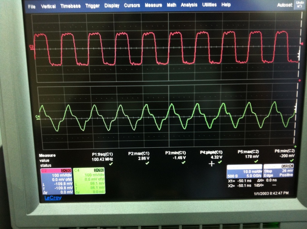
    01 - DAC_In_0x000_0xFFF___C2_IoutA2_Gnd____C4_IoutA2_IoutA1.jpg

    The DAC is driven with "All High" and "All Low" switched at 200 MHz. The C2 plot is the output of the J2 connector. The C4 plot is the output between the J2 center and J1 center.

    2.

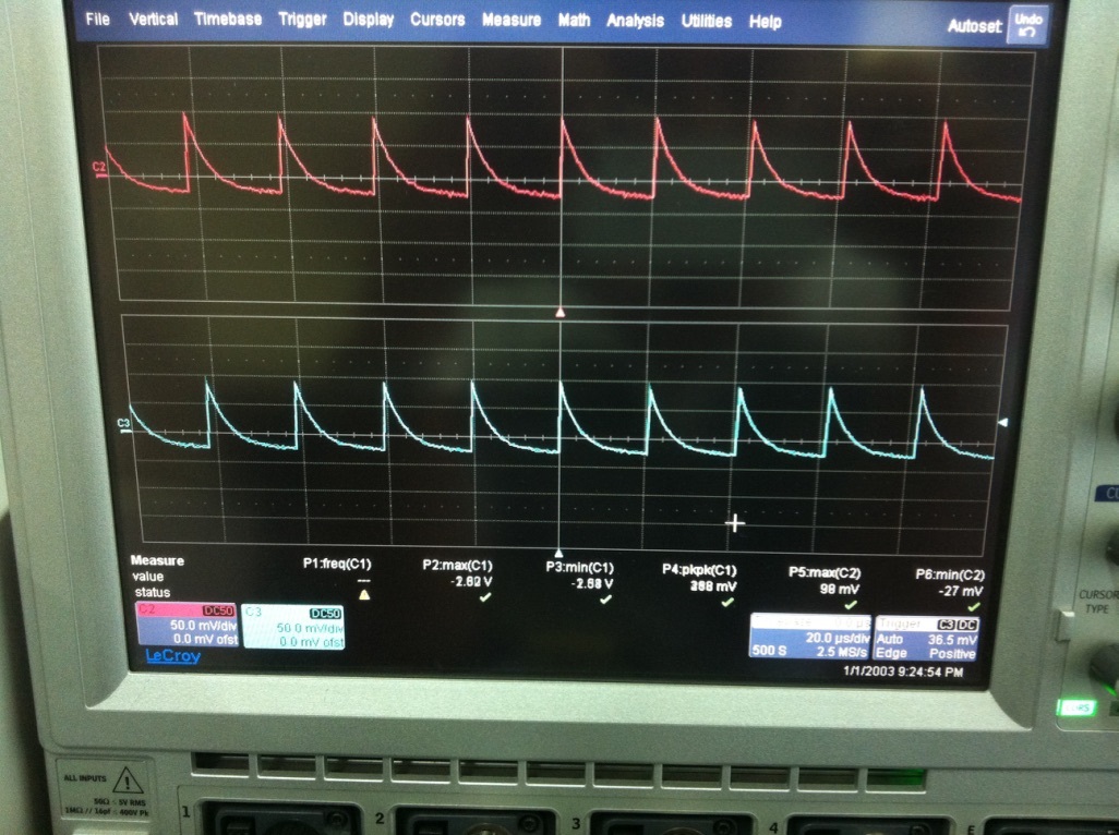
    03 - DAC_In_Ramp___C2_IoutA2_Gnd____C3_IoutB2_Gnd.jpg

    The DAC is driven with a RAMP input values. C2 is the output at the J2 and C3 is the output at J3.

    3.

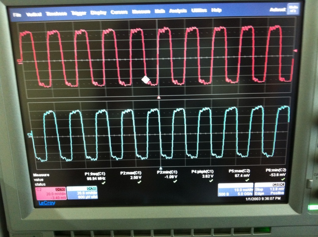
    05 - DAC_In_0x000_0xFFF___C2_IoutA2_Gnd____C3_IoutB2_Gnd.jpg

    The DAC is driven with "All High" and "All Low" at 200MHz. C2 is the output at J2 and C3 is the output at J3.

    Kindly let me know if these are the expected output levels.