This thread has been locked.

If you have a related question, please click the "Ask a related question" button in the top right corner. The newly created question will be automatically linked to this question.

ADS5562EVM: ADS5562evm: DC coupling input

Part Number: ADS5562EVM
Other Parts Discussed in Thread: THS4509, ADS5562

Hello all,

We need to be able to DC couple a single-ended signal in a ADS5562EVM, but it is AC coupled. Is there any modification that can be done to the board to achieve this? Strongly prefer not to make a new board and just modify this one.

Thanks,

PTD

  • Hi,

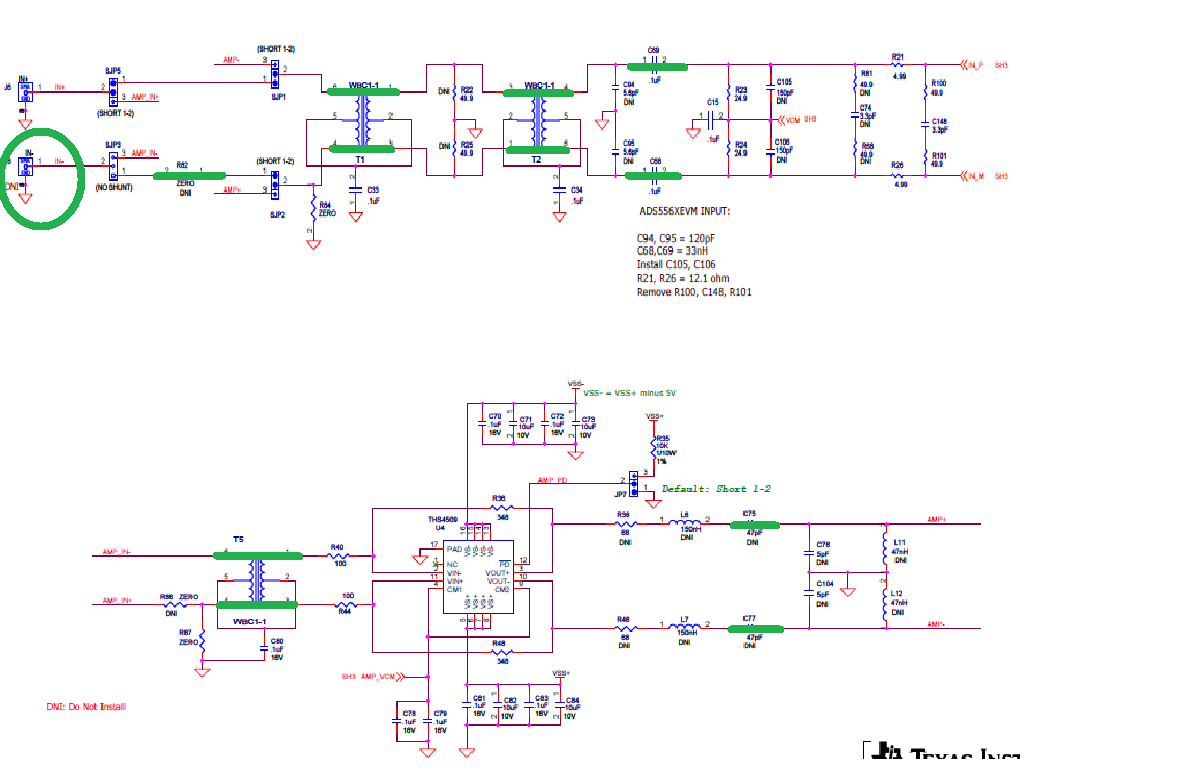
    If you wish to bring in an external signal that is DC coupled, then the signal would have to be already a differential signal that is biased to the desired level to match the ADC's VCM voltage.   In this case, you would have to solder in the second SMA connector for the other side of the differential signal, and solder in zero ohm resistors in place of the transformers and AC coupling caps, as such:

    The other choice is to not solder in the second SMA connector, but instead change the jumpers SJP1,2,5 to steer the input signal to the THS4509 amplifier that is on the EVM and use the amp to do the single ended to differential conversion.  You would still have to short out the transformers and AC coupling as in the above figure, but also short out the transformer and AC coupling caps around the amp as in the following figure.  The VCM voltage comes from the ADC to the CM input of the amp to set the biasing of the differential signal.  You would also have to design the resistors around the amp to get the gain that you want, and the pads for the R and L and C components after the amp are bare so that you could design your own anti aliasing filter after the amp.  If you chose to go with this option the amplifier forum would probably be the best place to get support on the amp design.

    Regards,

    Richard P.

    (The figures did not come through in the posting, so I saved them into an attachment.)

  • Hello Richard,

    Thanks for your help. Our input is not differential, so the second option makes the most sense.

    Richard Prentice said:
    The VCM voltage comes from the ADC to the CM input of the amp to set the biasing of the differential signal.

    If the input signal does not have an a priori known DC level, how can we handle that? I probably don't exactly understand the function of the VCM ADC and the CM amp pins, but I would want the DC level into the ADC to be that of the input signal itself. Is there some way to do that, e.g. using a bias tee or other configuration?

    Thanks,

    PTD

  • Hi,

    there was a similar question on this forum recently but with a different ADC.  https://e2e.ti.com/support/data_converters/high_speed_data_converters/f/68/p/606301/2232699#2232699  In that posting the question also was after doing a single ended to differential conversion, how to relate the DC level of the single ended input signal prior to the single ended to diff conversion to the amplitude of the diff signal after that conversion. 

    like in that other posting, you would have to design your signal conditioning such that your minimum single ended signal voltage is converted to a differential voltage that represents the minimum full scale input of the ADC, and such that your maximum input voltage of the single ended signal is converted to a differential voltage that represents the maximum full scale input of the ADC.     The VCM voltage has nothing to do with the amplitude of the signal - it is only the biasing of the differential signal. 

    copying from that posting and changing the numbers to reflect the full scale voltage definition of 3.56V for the ADS5562:

    If the differential input voltage to the ADC is such that the INP is at 0.89V below VCM and the INM is 0.89V above VCM, then the input differential voltage would be -1.78V and this would correspond to the lower limit of full scale and the output code would be all zero.   If  the INP is at 0.89V above VCM and the INM is 0.89V below VCM, then the input differential voltage would be +1.78V and this would correspond to the upper limit of full scale and the output code would be all ones.  So the range of input would be +/- 1.78V around VCM or 3.56V peak to peak.    You would need to design your input conditioning circuit such that your minimum input signal would be transformed to the -1.78V differential input to the ADC.   And your maximum input signal would be transformed to the +1.78V input to the ADC.   Then you would know what your input signal was when it was sampled and turned into the output code.

    Note that what VCM actually is in the above description does not affect what the differential input voltage is, only where the signal is biased to.

    Regards,

    Richard P.