This thread has been locked.

If you have a related question, please click the "Ask a related question" button in the top right corner. The newly created question will be automatically linked to this question.

ADS1610: Group Delay of ADS1610

Part Number: ADS1610

Hello HSADC team,

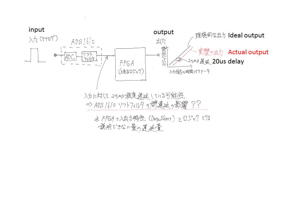
I have 2 questions about Group Delay of ADS1610.

Now customer is using ADS1610 but they facing a problem that ADS1610 seems to have around 20us group delay.

1. As I can see in datasheet page.4, typical value of group delay is 3us@fCLK60MHz.

    If fCLK is 50MHz, How much is the Group delay? 

2. As I can see in datasheet page.19, reccomended RBIAS resistor values for Different fCLK are like below.

If actual fCLK and RBIAS are different from this reccomentation list, Can this effect the Group delay value?

Thanks,

Yuta Kurimoto

  • Hello Kurimoto-san,

    Thanks for your question.

    The group delay in a delta-sigma ADC is the time for an analog input to appear in the digital output of the ADC. Group delay depends on the clock frequency, digital filter architecture, and oversampling ratio (OSR) and is usually expressed as a number of conversions.

    The group delay for the wideband FIR filter in the ADS1610 is specified in the Electrical Characteristics table for MODE = 00 as 3 x (60MHz/fCLK) us. This equates to 30 conversion periods for a data rate of 10MSPS.  For CLK = 50MHz, the group delay is still 30 conversions, but this now equates to 3.6us as the data rate reduces to 8.3MSPS.

    However, the remaining MODE settings use a different OSR and I do not see a clear specification for the group delay with those settings. Please allow me to discuss this further with the designer.

    The RBIAS resistance values in Table 5 are recommended based on the expected analog performance of the ADS1610. As the modulator sampling frequency is increased, more bias current is needed by the analog circuitry to achieve the specified performance. RBIAS should have no effect on the group delay in the digital filter, but I will confirm this as well.

    Best Regards,

  • Hello Ryan,

    Thanks for your detail answer.

    I'm looking forward to getting answer from you after your confirmation.

    Thanks and best regards.

    Yuta Kurimoto

  • Hello Ryan,

    Let me add one question.
    Is there any other factor which affect group delay except fCLK?
  • Hello Ryan,

    Could you please tell me any update for this?

    Thanks,

    Yuta Kurimoto

  • Hello Kurimoto-san,

    Sorry for the delay, I have been looking for prior team members to help with this. I just received some preliminary digital design review documents, but the group delay is not explicitly given for different MODE settings. Therefore, I do not have any additional information to provide other than what is in the datasheet.

    Besides the CLK frequency and MODE setting, there are no other factors which affect the group delay.

    Can you give us more information about the exact clock frequency and MODE setting? And how do they measure the group delay?

    Best Regards,
  • Hello Ryan,

    Thanks for your reply.

    Now I'm checking the MODE setting and measurement environment...

    Yuta Kurimoto

  • Hello Ryan,


    Thanks for your support. I got the MODE setting and measurement environment from customer.

    The mode setting of customer is 00. How much group delay change for each MODE setting?


    And below picture is their measurement environment. They looked the output data at not ADS1610 node but FPGA output node.

    They saw actual output is 20us delayed compared with ideal output. They guessed this delay is caused by ADS1610 soft filter. Do you know any idea about measurement method for group delay of ADS1610?


    Thanks!

    Yuta Kurimoto


  • Hi Kurimoto-san,

    Thank you for the update.

    What is the master clock frequency?

    As I mentioned previously, group delay for MODE = 00 is given as a typical spec in the Electrical Characteristics table as tGD = 3us x (60MHz/fCLK). I have limited documentation about the digital design, so I cannot say with any certainty what the group delay will be for other MODE settings. Does your customer need to know the group delay for other MODE settings?

    One important point: the group delay should be measured with an input step voltage at a known moment in time. The customer will need to have precise control over the input step. I don't believe the FPGA should introduce significant delay time, so probing the output of FPGA should be ok.

    How does the customer provide the input step voltage to the ADS1610?

    Best Regards,
  • Hello Ryan,

    Thanks for your answer.

    Master clock frequency is 50MHz.

    So I estimate the group delay should be 3us * (60MHz/50MHz) = 3.6us.

    However customer also would like to know the group delay for other MODE setting.

    Regarding with input step voltage, I'm checking with customer.

    Do you have any material how to measure the group delay of A-D converter?

    Thanks,

    Yuta Kurimoto

  • Hello Kurimoto-san,

    The best approximation that we can offer is that the group delay for each of the MODE settings should equate to ~1/2 the settling time listed in Table 4.

    Best Regards,
  • Hello Ryan,

    Thanks for your answer. That make it sense.

    Yuta Kurimoto