This thread has been locked.

If you have a related question, please click the "Ask a related question" button in the top right corner. The newly created question will be automatically linked to this question.

ADS4149EVM: Input Frequency not found

Part Number: ADS4149EVM

Hi,

I'm new to these EVMs.  I have ADS4149EVM Rev B, TSW1405EVM Rev C, and the GUI HSDC Pro v4.70.  I followed the ADS4149EVM setup instructions as best I could (it shows the TSW1200 and its 2p0 BETA, not the TSW140x or HSDC Pro v4.70).  Please help me with getting started.

ADS4149EVM jumpers are as in Table 1 (no amplifiers).  3.3V (50mA) to J16/J12 for on-board voltage regulators.  USBs from PC to each 'EVM.  One GUI window on PC.

Clock = 24.576 MHz sine, 1.5Vpp 0V offset.

Ain = 10 MHz sine, 1.3Vpp 0V offset.

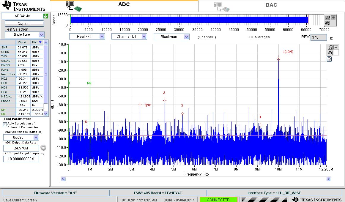
GUI lower left = test parameters:

samples = 64k

ADC output data rate =103M

ADC input Target freq = 10M

Downloaded Firmware to '1405 and the '1405's LED is ON.  When the Ain is off, the "Capture" codes = 8,242 to 8,251 (8,192 is ~ideal?  Vcm=0.9648V), "Real FFT" shows f1=113k at -113dBFs.  These seem OK.

When Ain=ON, the "Capture", the codes range from 4,237 to 12,266 (seems OK).  However, the "Real FFT" (Blackman) shows nothing at 12.576MHz (f1=42M, F2=19M, f3=22.7M, f4=38M, f5=3.6M)

Why nothing at 24.576MHz?  Am I doing something wrong with voltages, frequencies, or settings? 

  • Hi Rick,

    Can you please send the time domain data to me by choosing 'Save Raw ADC code as Binary File' option in File tab on top left corner of HSDC-Pro GUI?

    Regards,

    Sourabh

  • Sourabh,

    I overlooked some of things, which I have since corrected:

    1) the GUI's lower left "ADC Output Data Rate" must = the board's clock frequency

    2. The GUI's "ADC Input Target Frequency" must = the frequency of the signal being sampled

    3) Nyquist (frequencies of clock >= 2*signal)

    Please correct me if I have something incorrect.  So after changing clock to 25MHz and updating the GUI's lower left,

    Ain = 10MHz 1.3Vpp, it's working OK.  SNR ~50dB and ENOB ~8 (way below typical spec's of 71.9 dB and 11.3 bits; binary file attached).  These were much improved with lower frequency and amplitude  With

    Ain =  1MHz 0.2Vpp, SNR ~65dB and ENOB ~10.

    Any insights why (for a constant frequency) a lower amplitude improves SNR and ENOB?

    Rick

    ADS4149 Ain=1_3Vpp 10MHz.zip

  • Hello Rick,
    I looked at the binary files you attached. There are a few things which may have gone wrong:
    1. Provide a coherent frequency to analog inputs: When input signal frequency is 'coherent' with sampling clock frequency, it falls exactly on one of the bins in FFT. This avoids smearing of signal power to nearby bins. This also enables you to see an 'unwrap' wave which is nothing but the frequency bin of input signal in FFT shifted to bin#1 - so it's input signal with rearranged phase. The 'unwrap' wave is a useful way of finding if the sine wave (input signal) was properly sampled by ADC and correctly received by the FPGA. Ideal 'unwrap' wave should show one cycle of sine wave in complete sample set with no glitches along with a noise waveform overriding it. To know the value of coherent frequency for a given sample set, you may click 'Auto Calculation of Coherent Frequencies' and then set input signal source to this value. Then select 'time domain' entry in Test Selection drop down, and click on 'Overlay Unwrap Waveform'. You should be able to see a clean sine-wave with just one cycle in entire sample set. When input frequency is coherent to sampling clock frequency, it finishes integer number of cycles in given sample set, this simple rectangular window should be sufficient for processing FFT (don't need Blackmann, Hanning, or Hamming window).
    2. Use band-pass filter to filter out noise and harmonics from input signal source and from sampling clock source. In out testing of ADC's performance with sine-wave sources, we use TTE's band-pass filters with 3% pass-band of center frequency.
    3. Apply correct settings. If there are any power-up settings recommended, make sure you apply them using device GUI.
    4. Use ADC's internal digital patterns to ensure that digital link between ADC and receiver(FPGA) is robust. You can use Ramp test patterns of ADC which usually increments by 1 LSB of ADC every clock cycle.
    Let me know if you still struggle to get the proper performance.
    Regards,
    Sourabh