This thread has been locked.

If you have a related question, please click the "Ask a related question" button in the top right corner. The newly created question will be automatically linked to this question.

DAC3162: Output Delay issue between ‘DACA’ and ‘DACB’

Part Number: DAC3162
Other Parts Discussed in Thread: DAC3484, THS3217

Hello,

My customer is using DAC3162 (500Msps) and faced with below issue. Please help to get answer asap. They hope to get answer by tomorrow due to PCB OUT schedule.

In their system, ‘LVDS Lcoslk 120MHz’ in attached block diagram is shared by DAC3162 and LCOS display.

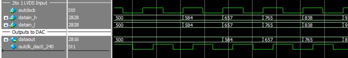
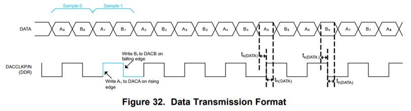
And the LCOS panel needs to get aligned analog output signal ‘DACA’ and ‘DACB’ of DAC3162 to get clear image (1080p 120fps), but the output image is distorted by output of DAC3162 due to delay between processing time of DATA A and B as described in Figure 32 as below capture.


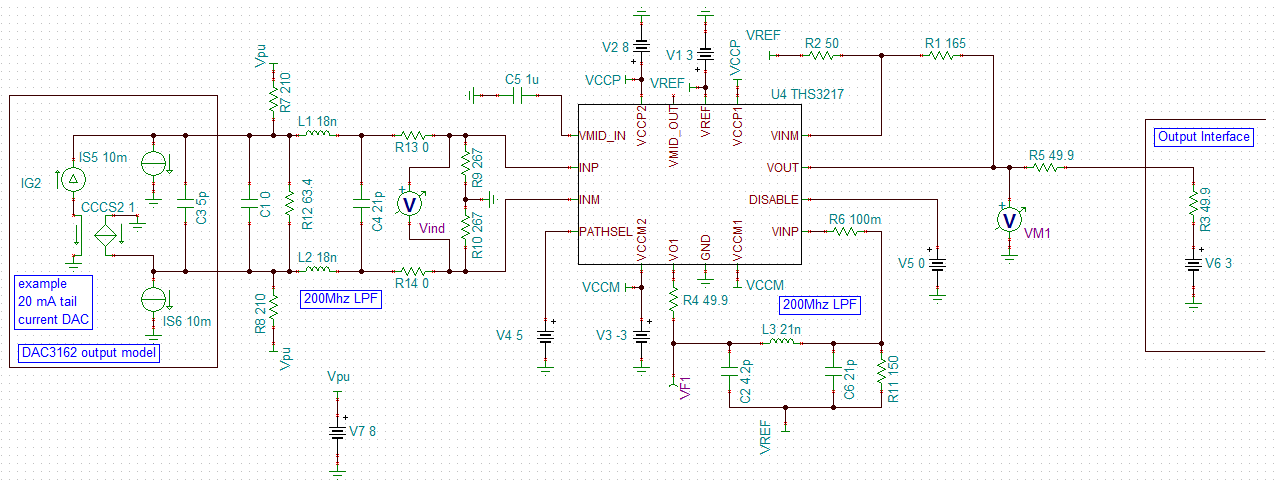
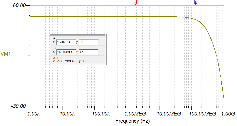
Another issue is that output range of IOUTP and IOUTN is too low about 0.5V. LCOS panel needs to get 0V to 6V peak to peak. So they are using external OPAMP (MAX228) to amply output about 12 times of DAC. They hope to get answer how to increase output level of DAC3162 and application note to get 0V to 6V analog output.

They also hope to get suggestion for 1Gsps Dual-Channel DAC if this issue can be solved.


1.  We are using two channel output DAC3162. We just noticed that analog output port A and B has half clock phase off.

    For our application, the output of port A and B should be aligned.

    Please let us be advised how we can resolve this issue.


2.    The output range of DAC3162 is 0.5Vpp with DC offset voltage.

    We need to amplify the DAC output signal from 0.5Vpp to 6Vpp of 0V to 6V swing with 3V bias voltage.

    Could you any suggestion of application circuits for getting the 6Vpp?

Best regards,

Shaka Lee

  • Shaka,

    Have the customer swap A data with B data and see how this effects the skew. By design, the part should have both channels output the same samples at the same time. Even though the data is clocked in at different times, the internal clocking will adjust for this.

    Regards,

    Jim 

  • Hi Jim,

    Thank you for your answer. They already tried to swap A data and B data, but the result was same. Could you please let me know detail for adjust timing with internal clocking? There is no information in datasheet. Could you advise what we can do more with current HW?

    As below simulation of 2 channel to 1 channel LVDS buffer in FPGA, FPGA outputs same data on A and B. Output clock is shifted 90 degree in this simulation.

    They also considering DAC3484 to replace DAC3162, if this issue is not fixed. Is there any way to adjust or make delay of DAC outputs separately?

    Best regards,

    Shaka

  • Hi Shaka,

    I am working on the DAC3162 output amplification from 0.5Vpp to 6Vpp, and should be back with a solution soon.

    Best Regards,

    Rohit 

  • Hi Shaka,

    I think the below THS3217 circuit could be used to amplify the DAC3162 output from 0.5Vpp to 6Vpp. On the left side box is the DAC3162 output model giving 0 to 20mA output current with 5pF output capacitance.

    There is a 170MHz DAC re-construction Bessel filter in-between the DAC3162 and THS3217 in-order to filter out the DAC harmonics. I believe for 1080p 120fps, the signal chain BW required is ~140MHz. So, 170MHz BW in the filters should be good enough. However, if that's not the right BW, let me know and we can tweak the L and C values to get the correct BW.

    The other thing is that if you are planning to use the DAC3484 instead of the DAC3162, then the interface circuit to the THS3217 will change. 

    Best Regards,

    Rohit

    Transient Response:

    Frequency Response: