This thread has been locked.

If you have a related question, please click the "Ask a related question" button in the top right corner. The newly created question will be automatically linked to this question.

ADS5231EVM: over current limitation after burn-in test

Part Number: ADS5231EVM

We bought a ADS5231EVM card. Connect with the default instructions.

3.3-V ADC output buffer supply to J17 and return to J18.
3.3-V ADC analog supply to J11 and return to J10.
Use a function generator with 50-W output to input a 45-MHz, 1.5-V offset, 3-V square-wave signal into
J3.
Use frequency generators with a 50-W output to provide a 10.1-MHz, 0-V offset, –1-dBFS amplitude,
sine-wave signal into J15.

At first, ADS5231EVM works well as the following picture. Fetched data are reconstructed into decimal sinusoidal waveform correctly.

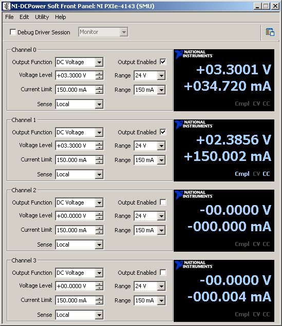
After 1 week, the power supply reveals into 'cc' condition. The ADC core power seems okay.
But the output buffer current reached 150mA as the following picture. The clock out pin failed to trigger logic analyzer.

Does any one have any ideas about this phenomenon?

Thank you for any help.

  • Hi Den Chao,

    We are taking a look into this, and will be back with you shortly.

    Regards,

    Dan
  • Den,

    In the post, you mention burn-in test. Was this board placed in a temp chamber? If so, how hot did you get it? These boards were not designed for temperature testing. Did you remove power and test for a short on the buffer power supply on the board? If a short does exist, you may want to try cleaning the area around the two buffer devices. There may be some flux build up that has created this short. I would suggest using an ultra-sonic cleaner if you have one available.

    Regards,

    Jim

  • We just planed to start the burn-in test. The temperature is set at 25 degree Celsius and the PCB is kept on running for one week.

    Thank you for the reply

    Best Regards,

    Den