This thread has been locked.

If you have a related question, please click the "Ask a related question" button in the top right corner. The newly created question will be automatically linked to this question.

ADS1282: PGA block diagram of ADS1282

Part Number: ADS1282
Other Parts Discussed in Thread: REF6050

Hi all,

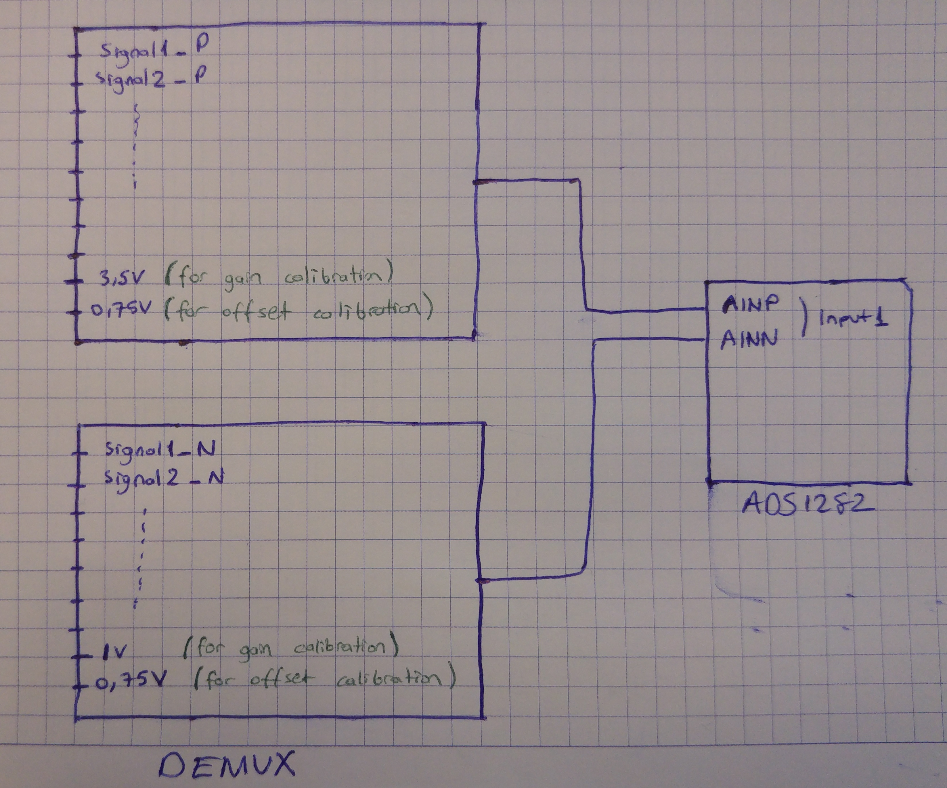
I have some questions about PGA block diagram in ADS1282 datasheet. As i understood from the datasheet, there is following circuit in the ADC. Am i right?

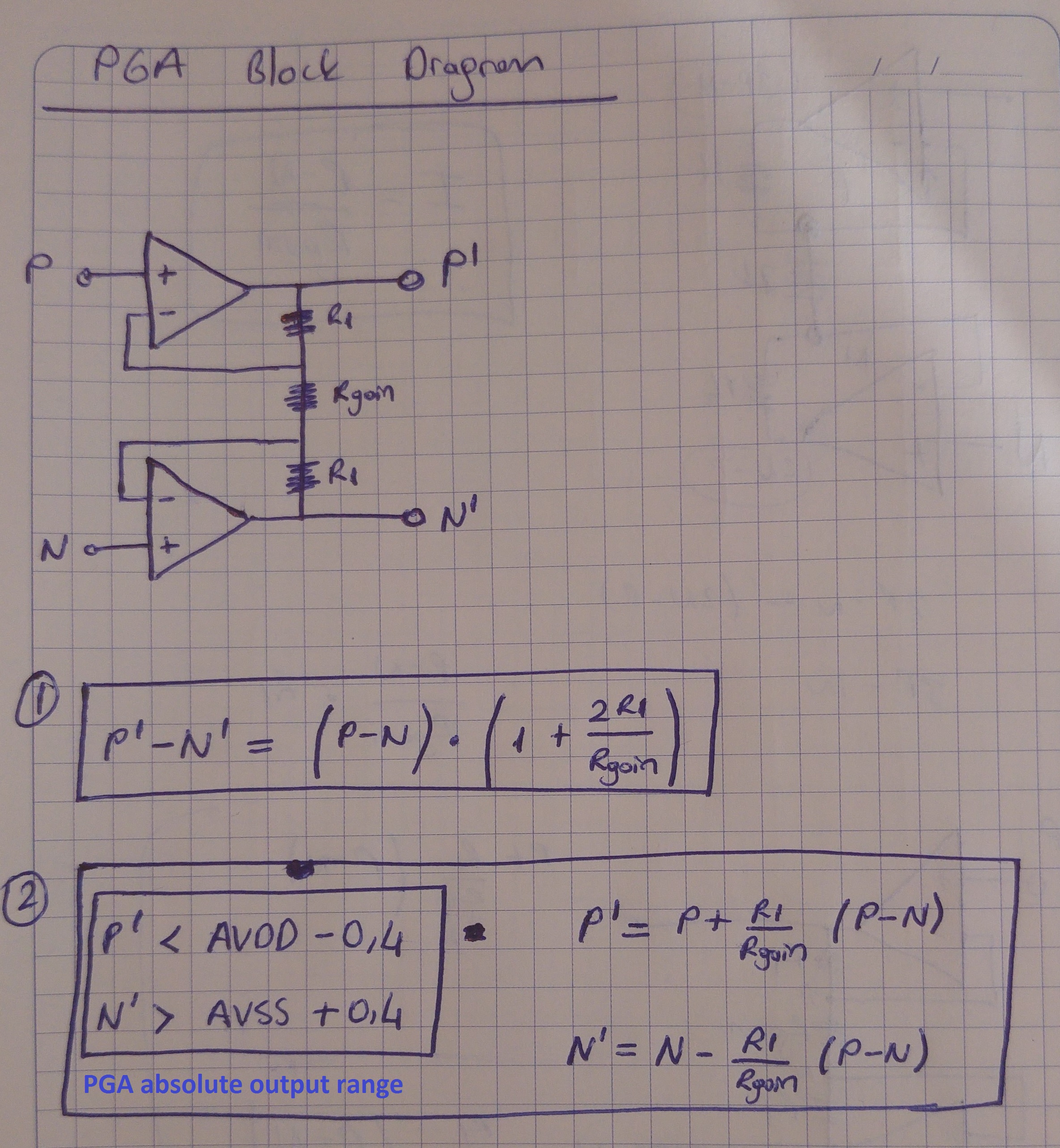
If i think wrong, please share correct PGA circuit. According to correct PGA circuit, i will adjust analog inputs or adjust gain for appropriate PGA output range.

Regards,
Eren

  • Hi Eren,

    Your schematic is correct. It corresponds nicely with Figure 29 in the ADS1282 datasheet.

    While I believe your calculations are correct, you also need to be mindful of the input voltage limitations, as they are a bit more restrictive than the output swing to the rails limits. If you satisfy the conditions below, you shouldn't run into any common-mode range limitations.  

    Best regards,
    Chris

  • Hi Chris,


    I have a last additional question. I think to use following circuit for gain and offset calibration. I aim to calibrate the contribution of multiplexer to gain and offset error. Do you recommend this circuit? (ADC is in unipolar mode, AVDD=5V, AVSS=0V, VREF=5V and PGA is 1.)


    Best regards,

    Eren

  • Hi Eren,

    In your circuit, do the DEMUX blocks refer to external multiplexers or are you drawing the ADS1282's MUX and ADC functional blocks separately?


    Your calibration voltages appear to be correct:

    • AINP = AINN = 0.75V for offset calibration (I assume these are coming from the same source to ensure they match), such that Vin = 0V. Just make sure to perform offset calibration before gain calibration. 

    • AINP = 3.5V and AINN = 1V, such that Vin = 2.5V for gain calibration (I assume that you are using a 5V reference so that +FS = 2.5V). This is provides a common-mode voltage of 2.25V, nearly centered at the middle of the input range (2.1 V common-mode). Just make sure that these calibration voltage sources have better accuracy than the ADS1282's typical gain error, otherwise they may actually make the gain error worse after calibration.


    Best regards,
    Chris

  • Hi Chris,

    Firstly, DEMUX blocks are refer to external 32 channel analog multiplexers. Actually there are four multiplexers. The first two are for input 1, the other two are for input 2. I only drew the first two multiplexers which are for input 1.

    Secondly, AINP = AINN = 0.75V (These are coming from the same source)

    Thirdly, gain calibration circuit is below. According to my calculation, total gain error is 310uV. Are there any recommandations for this circuit?

    Fourthly, ADS1282 datasheet states that gain error after calibration is 0.0002%. I am wondering how to calibrate at this accuracy?

    Best regards,
    Eren

  • Hi Eren,

    The above circuit looks alright; however, do note that the accuracy of the LM4050 (A grade) will be on the order of 0.1% at room temp; so the reference source may contribute more error than the resistor divider and buffer circuit.

    ....Something like the REF6050 would be closer to 0.05% accurate and could double as the ADC's reference source.


    The "0.0002%" gain error after calibration specification has a foot note that says, "Calibration accuracy is on the level of noise reduced by 4 (calibration averages 16 readings)". This is a mathematical limit placed on the gain error due to the ADC's noise. It assumes a perfect calibration source, so in practice the actual gain error after calibration will be higher due to the error and noise from the calibration source.


    Best regards,
    Chris
  • Hi Chris,

    Thanks for your answer.

    Best Regards,

    Eren