Because of the Thanksgiving holiday in the U.S., TI E2E™ design support forum responses may be delayed from November 25 through December 2. Thank you for your patience.

This thread has been locked.

If you have a related question, please click the "Ask a related question" button in the top right corner. The newly created question will be automatically linked to this question.

ADS54J54: The spur about ADS54J54

Part Number: ADS54J54

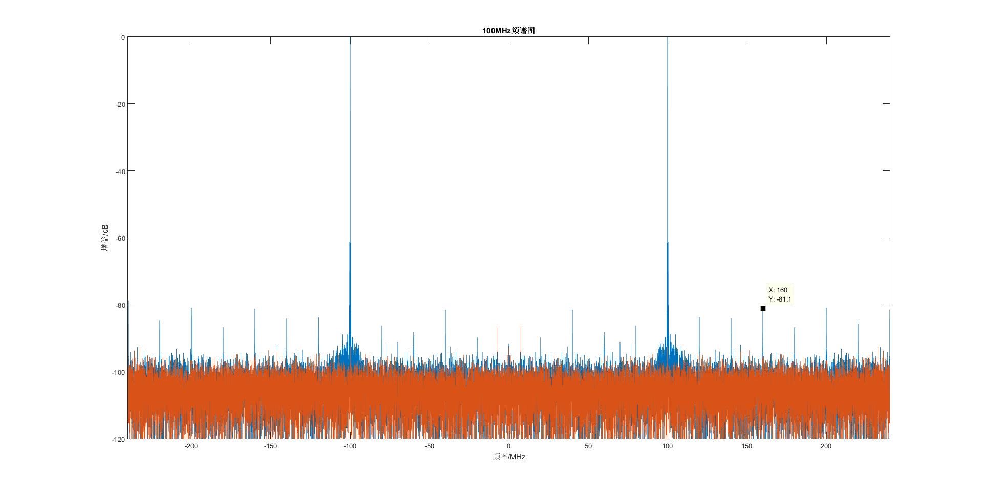
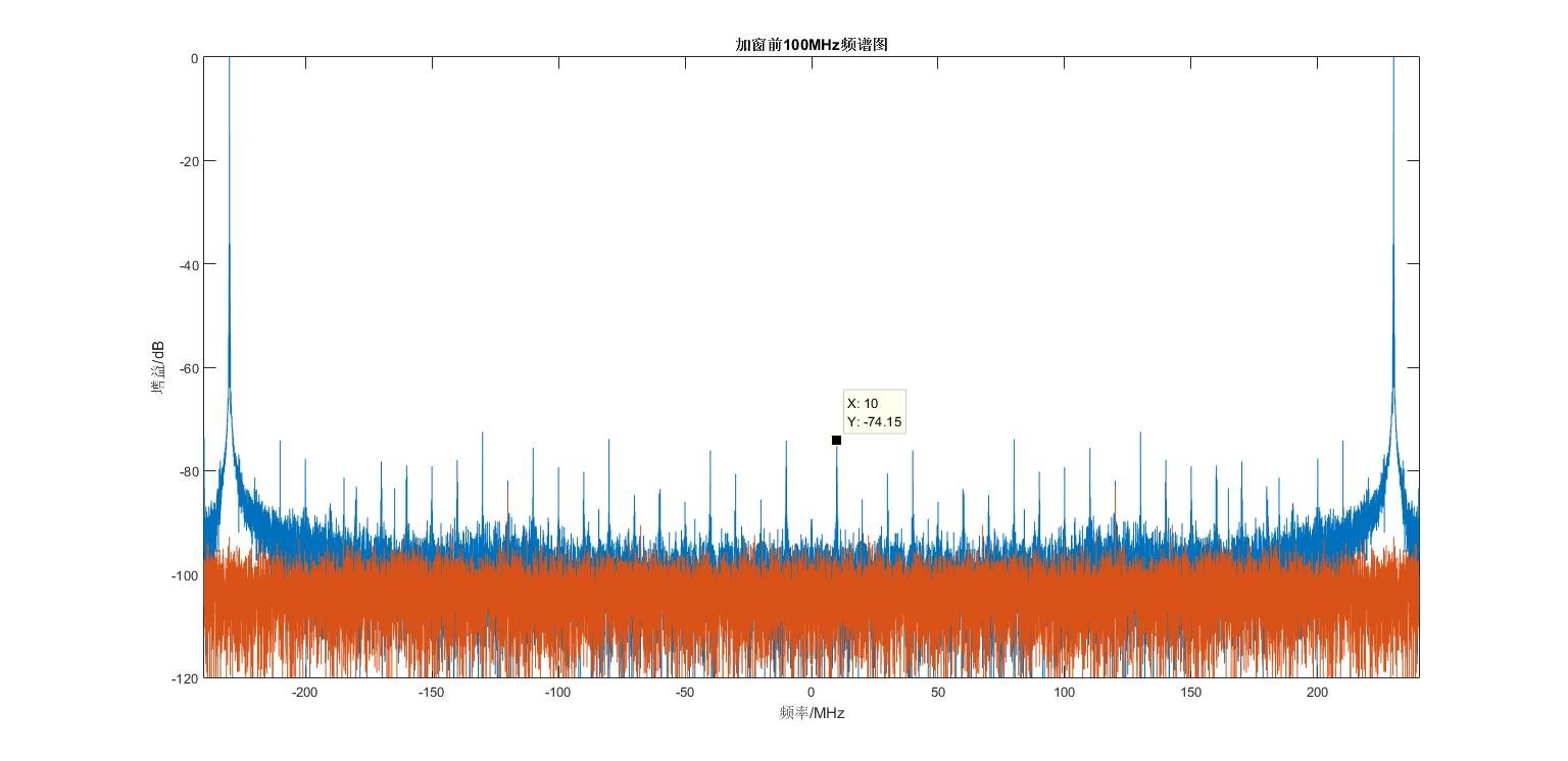
I test the SFDR of ADS54J54 on my own sample PCB board. The sample rate is 480Mhz, and the frequency of the input  sine waveform are 10MHz, 100MHz and 230MHz. The SFDR of 10MHz is okey. But there are many spur component when the frequency are 100MHz and 230MHz. And the location of the spur between -fs/2~fs/2  are  (M*Fs-/+ N*fin) . I think these spur are folded from the other nyquist feild. But I don't know why.

I take some notice into account as follows when I test the ADS54J54.

1. I insert a bandpass filter in the analog input of the ADS54J54. Central freq = 100MHz/230MHz. BW = 10MHz. The restrain at HD2 and HD3 are greater than 60dB. The amplitude of higher-order harmonic measured through spectrum analyzer are very small. So I don't think the spur come from the input sinewave.

2. I power down LMK04828B's SYSREF output after the JESD204B established.

3. I sample the noise of the PCB board , there are no other coupling freqency signal.

Now the SFDR of 100MHz is a little better but not perfect, SFDR=81.1dB. The SFDR of 230MHz is terrible. SFDR = 74.15. I realy don't konw where the spur comes from.

  • Hi Zhipeng lv,

    We are taking a closer look at your question, and will be back with you soon.

    Best Regards,

    Dan
  • Zhipeng,

    Are you enabling the decimation filters? If so, are you using low pass mode or high pass mode for these inputs?

    Regards,

    Jim

  • Jim

    I don't enable the decimation filter. The sample rate is 480MHz and the single lane rate is 4.8Gbps. JESD204B parameter: HD =1 LMFS = 4211

    Regards,

    Zhipeng
  • Can you send the complete register configuration you are using?
  • Jim

       I'm sorry to reply you late. The  configuration is in the attachmeant. And I find a point making my spur performance better. In the begining I design the input device circuit as the datasheet and the ADS54J54EVM. The  unbalancedness between P/N of the Balun is very obvious. and  the spur performance is just like the result described in my firs post.  Then I attempt to remove the bypass 0.1uF capactance between two 25ohm resistance. The unbalancedness between P/N takes a turn for better. And the spur performance about 230MHz becomes a little better compared with the result in my first post. Most of spurs are below -85db except 20MHz(-79db), 210MHz(-78.96db), 190MHz(-74.65db). These three frequency component may be the second, third, fifth harmonic reflexed in the first Nyquist feild. The sample rate is 480MHz.

    20MHz : -480MHz + 460MHz = -20MHz;   210MHz : -480MHz+ 690MHz = 210MHz

    190MHz: -960MHz + 1150MHz = 190MHz;

    So how to remove the spur at 20MHz,190MHz,210MHz. And why dose the 0.1uF capactance have influence on the spur performance and the unbalancedness. Whe do I remove it the spur performance and the unbalancedness are better.

    Thank you !

    configuration.txt
                       0:	begin    Areg <= 7 'h0D;Dreg <=16'h0000;end                //JESD RESET AB/CD = 0 JESD INIT AB/CD = 0                                                                                                                      
                      64:   begin    Areg <= 7 'h0D;Dreg <=16'h0202;end                //JESD INIT  AB/CD = 1
                     128:   begin    Areg <= 7 'h0D;Dreg <=16'h0303;end                //JESD RESET AB/CD = 1
                       
                     192:   begin    Areg <= 7 'h00;Dreg <=16'h4000;end                //3 wire SPI / offset binary / decimation filter disable / 
                     256:   begin    Areg <= 7 'h01;Dreg <=16'h2F7A;end                //OVRA THRESH AB/CD = 111       FOVR LENGTH AB/CD = 4 clock cycle    
          
                     320:   begin    Areg <= 7 'h03;Dreg <=16'h0040;end                 // clock for channel CD = CD divider source  clock for channel AB =                                                                                         AB clock source
                                                                                        // SYSREF_CD  = use sysref AB inputs  clk_div = 1
                     384:   begin    Areg <= 7 'h04;Dreg <=16'hC00B;end                 //OVRA OVRB ENABLE OVRC OVRD disable  SYSREF AB/CD input 0 - delay
                                                                                        // SYNC AB enable  SYNC CD disable
                                                                                        
                     448:   begin    Areg <= 7 'h05;Dreg <=16'h00DA;end                 //light sleep channel AB =1  light sleep channel CD = 0 
                                                                                        //TEMP sensor = 1 clock buffer = 1 clock divider channel AB = 1                                                                                        clock divider channel CD =0
                                                                                        // Buffer SYSREF AB = 1   Buffer SYSREF CD = 0
                                                                                        
                     512:   begin    Areg <= 7 'h06;Dreg <=16'hFFFF;end                 //POWER DOWN MODE through SPI
                     // step
                     576:   begin    Areg <= 7 'h07;Dreg <=16'h0144;end                // ��ʱ�ӷ�Ƶ�ȵ�ʱ����
                     640:   begin    Areg <= 7 'h08;Dreg <=16'h0144;end                // ��ʱ�ӷ�Ƶ�ȵ�ʱ����
                     704:   begin    Areg <= 7 'h0C;Dreg <=16'h31C2;end                // channel CD don;t use sysref   channel AB use only the next one
                     768:   begin    Areg <= 7 'h0E;Dreg <=16'h000F;end                // channel AB enable / channel CD disable 
           //JESD204B parameters AB          
                     832:   begin    Areg <= 7 'h0F;Dreg <=16'h0001;end                // channel AB F =1  M =2
                     896:   begin    Areg <= 7 'h10;Dreg <=16'h03A3;end                // K = 32 L = 4
                     960:   begin    Areg <= 7 'h13;Dreg <=16'h0020;end                // SYNCbAB input non - invert HD =1 SCRAMBLE MODE DISABLE
           
           //JESD204B paramater CD
                    1024:  begin     Areg <= 7 'h16;Dreg <=16'h0001;end                //  channel CD F =1  M =2              
                    1088:  begin     Areg <= 7 'h17;Dreg <=16'h03A3;end                //  K = 32 L =4
                    1152:  begin     Areg <= 7 'h1A;Dreg <=16'h0020;end                //  SYNCbCD input non - invert HD =1 SCRAMBLE MODE DISABLE
           
                    1216:  begin     Areg <= 7 'h1D;Dreg <=16'h0000;end                // test pattern disable / normal operation
                                 
           // JESD204B power down mode
                    1280:  begin     Areg <= 7 'h1E;Dreg <=16'h010F;end                //JESD PLL channel CD power down  Channel CD power down   
                    1344:  begin     Areg <= 7 'h1F;Dreg <=16'hFFFF;end                //JESD204 power down mode
           
                    1408:  begin     Areg <= 7 'h20;Dreg <=16'h0000;end                //lane non - invert / don't output PRBS pattern
                    1472:   begin    Areg <= 7 'h21;Dreg <=16'h0000;end                //PRBS pattern  Full scale is 1.25Vpp      
    
          // pre_emhasis           
                    1536:  begin     Areg <= 7 'h64;Dreg <=16'h0000;end                // pre_emphasis disable AB
                    1600:  begin     Areg <= 7 'h67;Dreg <=16'h0000;end                // pre_emphasis current AB
                    
                    1664:  begin     Areg <= 7 'h68;Dreg <=16'h0000;end                // pre-emphasis disable CD                              
                    1728:  begin     Areg <= 7 'h6B;Dreg <=16'h0000;end                // pew_emphasis disable CD
          // JESD INITIAL AGAIN
                    1792:  begin     Areg <= 7 'h0D;Dreg <=16'h0202;end                //JESD RESET AB/CD = 0 
                    1856:  begin     Areg <= 7 'h0D;Dreg <=16'h0303;end                //JESD RESET AB/CD = 1                             
                    1920:  begin     Areg <= 7 'h0D;Dreg <=16'h0101;end                //JESD INIT AB/CD = 0    

  • Jim

       I'm sorry to reply you late. The  configuration is in the attachmeant. And I find a point making my spur performance better. In the begining I design the input device circuit as the datasheet and the ADS54J54EVM. The  unbalancedness between P/N of the Balun is very obvious. and  the spur performance is just like the result described in my firs post.  Then I attempt to remove the bypass 0.1uF capactance between two 25ohm resistance. The unbalancedness between P/N takes a turn for better. And the spur performance about 230MHz becomes a little better compared with the result in my first post. Most of spurs are below -85db except 20MHz(-79db), 210MHz(-78.96db), 190MHz(-74.65db). These three frequency component may be the second, third, fifth harmonic reflexed in the first Nyquist feild. The sample rate is 480MHz.

    20MHz : -480MHz + 460MHz = -20MHz;   210MHz : -480MHz+ 690MHz = 210MHz

    190MHz: -960MHz + 1150MHz = 190MHz;

    So how to remove the spur at 20MHz,190MHz,210MHz. And why dose the 0.1uF capactance have influence on the spur performance and the unbalancedness. Whe do I remove it the spur performance and the unbalancedness are better.

    Thank you !

    2211.configuration.txt
                       0:	begin    Areg <= 7 'h0D;Dreg <=16'h0000;end                //JESD RESET AB/CD = 0 JESD INIT AB/CD = 0                                                                                                                      
                      64:   begin    Areg <= 7 'h0D;Dreg <=16'h0202;end                //JESD INIT  AB/CD = 1
                     128:   begin    Areg <= 7 'h0D;Dreg <=16'h0303;end                //JESD RESET AB/CD = 1
                       
                     192:   begin    Areg <= 7 'h00;Dreg <=16'h4000;end                //3 wire SPI / offset binary / decimation filter disable / 
                     256:   begin    Areg <= 7 'h01;Dreg <=16'h2F7A;end                //OVRA THRESH AB/CD = 111       FOVR LENGTH AB/CD = 4 clock cycle    
          
                     320:   begin    Areg <= 7 'h03;Dreg <=16'h0040;end                 // clock for channel CD = CD divider source  clock for channel AB =                                                                                         AB clock source
                                                                                        // SYSREF_CD  = use sysref AB inputs  clk_div = 1
                     384:   begin    Areg <= 7 'h04;Dreg <=16'hC00B;end                 //OVRA OVRB ENABLE OVRC OVRD disable  SYSREF AB/CD input 0 - delay
                                                                                        // SYNC AB enable  SYNC CD disable
                                                                                        
                     448:   begin    Areg <= 7 'h05;Dreg <=16'h00DA;end                 //light sleep channel AB =1  light sleep channel CD = 0 
                                                                                        //TEMP sensor = 1 clock buffer = 1 clock divider channel AB = 1                                                                                        clock divider channel CD =0
                                                                                        // Buffer SYSREF AB = 1   Buffer SYSREF CD = 0
                                                                                        
                     512:   begin    Areg <= 7 'h06;Dreg <=16'hFFFF;end                 //POWER DOWN MODE through SPI
                     // step
                     576:   begin    Areg <= 7 'h07;Dreg <=16'h0144;end                // ��ʱ�ӷ�Ƶ�ȵ�ʱ����
                     640:   begin    Areg <= 7 'h08;Dreg <=16'h0144;end                // ��ʱ�ӷ�Ƶ�ȵ�ʱ����
                     704:   begin    Areg <= 7 'h0C;Dreg <=16'h31C2;end                // channel CD don;t use sysref   channel AB use only the next one
                     768:   begin    Areg <= 7 'h0E;Dreg <=16'h000F;end                // channel AB enable / channel CD disable 
           //JESD204B parameters AB          
                     832:   begin    Areg <= 7 'h0F;Dreg <=16'h0001;end                // channel AB F =1  M =2
                     896:   begin    Areg <= 7 'h10;Dreg <=16'h03A3;end                // K = 32 L = 4
                     960:   begin    Areg <= 7 'h13;Dreg <=16'h0020;end                // SYNCbAB input non - invert HD =1 SCRAMBLE MODE DISABLE
           
           //JESD204B paramater CD
                    1024:  begin     Areg <= 7 'h16;Dreg <=16'h0001;end                //  channel CD F =1  M =2              
                    1088:  begin     Areg <= 7 'h17;Dreg <=16'h03A3;end                //  K = 32 L =4
                    1152:  begin     Areg <= 7 'h1A;Dreg <=16'h0020;end                //  SYNCbCD input non - invert HD =1 SCRAMBLE MODE DISABLE
           
                    1216:  begin     Areg <= 7 'h1D;Dreg <=16'h0000;end                // test pattern disable / normal operation
                                 
           // JESD204B power down mode
                    1280:  begin     Areg <= 7 'h1E;Dreg <=16'h010F;end                //JESD PLL channel CD power down  Channel CD power down   
                    1344:  begin     Areg <= 7 'h1F;Dreg <=16'hFFFF;end                //JESD204 power down mode
           
                    1408:  begin     Areg <= 7 'h20;Dreg <=16'h0000;end                //lane non - invert / don't output PRBS pattern
                    1472:   begin    Areg <= 7 'h21;Dreg <=16'h0000;end                //PRBS pattern  Full scale is 1.25Vpp      
    
          // pre_emhasis           
                    1536:  begin     Areg <= 7 'h64;Dreg <=16'h0000;end                // pre_emphasis disable AB
                    1600:  begin     Areg <= 7 'h67;Dreg <=16'h0000;end                // pre_emphasis current AB
                    
                    1664:  begin     Areg <= 7 'h68;Dreg <=16'h0000;end                // pre-emphasis disable CD                              
                    1728:  begin     Areg <= 7 'h6B;Dreg <=16'h0000;end                // pew_emphasis disable CD
          // JESD INITIAL AGAIN
                    1792:  begin     Areg <= 7 'h0D;Dreg <=16'h0202;end                //JESD RESET AB/CD = 0 
                    1856:  begin     Areg <= 7 'h0D;Dreg <=16'h0303;end                //JESD RESET AB/CD = 1                             
                    1920:  begin     Areg <= 7 'h0D;Dreg <=16'h0101;end                //JESD INIT AB/CD = 0    

  • Zhipeng,

    Use a bandpass filter on your IF input.

    Regards,

    Jim