This thread has been locked.

If you have a related question, please click the "Ask a related question" button in the top right corner. The newly created question will be automatically linked to this question.

ADS7865: Internal parasitic capacitance

Part Number: ADS7865
Other Parts Discussed in Thread: OPA2836, OPA2301, OPA2365

Hi all

Would you mind if we ask ADS7865?
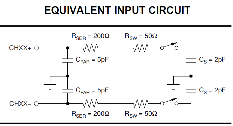
How much is the internal parasitic capacitance?
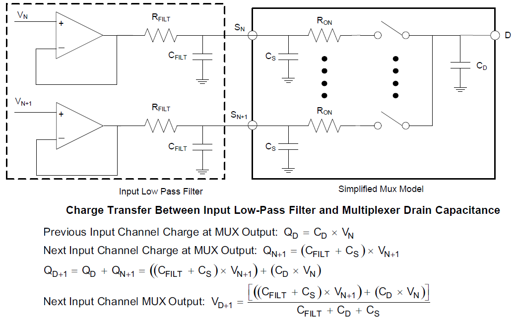
Our customer is worried about memory effect by changing channel at MUX.

In order to prevent from memory effect, if you have some advice, could you let us know it?

Kind regards,

Hirotaka Matsumoto

  • HI Hirotaka-san

    The ADS7865 is a SAR ADC.  The SAR ADC input needs to be driven with an external amplifier and RC filter that is able to re-charge the internal sample-and-hold capacitor and settle within the acquisition period.  The internal sample-and-hold capacitor of the ADS7865 is 2pF and the equivalent input circuit is shown on p5 of the datasheet.

    The internal sample-and-hold will tend to store the charge from the previous channel conversion, and the external amplifier driver circuit must be able to completely re-charge (or discharge) the 2-pF internal sample-and-hold capacitor within the 12-Bit resolution of the ADC during the acquisition period.  The acquisition period is a function of the sampling rate. 

    For example, when operating the device at maximum throughput of 2-MSPS, the acquisition time is ~65ns.  It is recommended that the device is driven with an external amplifier and RC filter with high enough Bandwidth and/or low output impedance to be able to settle within the resolution of the ADC during the acquisition period.  Therefore, using an amplifier with higher BW than >50MHz is recommended. 

    The OPA2365, OPA2836 and/or OPA2301 together with an optimally designed RC filter may be used to drive the ADS7865. 

    For detailed theory, explanation and TINA simulation examples on SAR ADC input amplifier driver design please review the TI Precision Labs ADCs: SAR ADC Input Driver Design:

    https://training.ti.com/ti-precision-labs-adcs#section-5

    Alternatively, if you require detailed suggestions for the amplifier and/or RC filter, please let us know the maximum sampling rate required in the application and all the details of the  mode of operation, (fully- differential or pseudo-differential) so we can propose a driving circuit.

    Best Regards,

    Luis Chioye
    PA ADC Applications

  • Luis san

    Thank you so much for your reply.

    The SAR ADC input needs to be driven with an external amplifier and RC filter that is able to re-charge the internal sample-and-hold capacitor and settle within the acquisition period. 
    ->We understand that SAR ADC input needs to be driven with an external amplifier and RC filter.
       They prevent from kick noise and help to charge Cs. 

    We would like to confirm memory effect again, could you refer to the attachment file?
    On the equivalent input circuit, each Cs are contained each inputs(CHXX+/CHXX-), our customer recognizes that it doesn't occur memory effect.
    Is this recognition correct?
    And then, Internal parasitic capacitance is so small value compared with CS. It doesn't matter, right?
    20180227_Memory effect.pdf

    Finally, at last, could you let us know follows;
    Are kickback noise and memory effect the same?

    We appreciate your help always.

    Kind regards,

    Hirotaka Matsumoto

  • Hello Hirotaka-san,

    The memory effect present in a discrete multiplexer application output drain capacitance (CD) is very similar to the effect on a sample-and-hold capacitor on a SAR ADC that has built-in multiplexer.   The figure below shows the charge transfer between the input low pass filter and a discrete multiplexer drain capacitance:

    The charge transfer effect on the ADS7865 is conceptually the same, in this case the sample-and-hold capacitor will store most of the charge from the previous channel conversion, and the external amplifier driver + RC kickback filter needs to be able to recharge the sample-and-hold on the allowed acquisition time (~65ns when using the ADS7865 at full throughput).

    In a discrete multiplexer, the mux output pin has a drain capacitance and a parasitic capacitance associated to the output pin ESD structure. In the case of the ADS7865, the internal multiplexer output is connected to the ADC (without any ESD structure parasitic capacitance), and the dominant storage capacitor is the 2pF sample-and-hold.

    When scanning through channels on the ADS7865, the charge kickback effect is primarily due to the charge stored from the previous channel conversion. The worst case occurs when the previous channel conversion has a voltage close to positive full-scale and the new channel has a voltage close to negative scale. The conservative approach is to design a driver circuit assuming that a full-scale step change has occurred between channels; where the driver circuit has to completely recharge/discharge the S/H during the acquisition time within the resolution of the ADC.

    If you require suggestion with the driver circuit and/or simulations, please let me know the maximum throughput required per channel and the mode of operation, i.e differential or pseudo differential, supply requirements, reference voltage, etc,

    Many Thanks,

    Kind Regards,

    Luis

  • Luis san

    Thank you so much for your cooperation always!
    Finally, we have two additional guestions.

    <Question1>
    How much are MAX and MIN value of S/H capaitor?
    Our customer would like to know as reference data.
    If you have some information, could you let us know?

    <Question2>
    Just in case, we would like to confirm.
    To configure external RC, our cusomer assumes that conversion accuracy might be inferior. 
    Or, does it occur another problem by addtion external RC?(we think there is no problem.)

    We appreciate your help always.

    Kind regards,

    Hirotaka Matsumoto 

  • Luis san

    We quess that your days are so busy, however could you let us know the reply for our last update?

    Kind regards,

    Hirotaka Matsumoto

  • Hi Hirotaka-san,

    - The datasheet does not guarantee a minimum or maximum value for the S/H capacitor. An estimate of the capacitance distribution over device and process variation would be 2pF±15% or 1.7pF to 2.3pF.

    - Using an RC filter at the inputs of a SAR ADC is standard practice.The external RC kickback filter needs to be designed in conjunction with the driver amplifier circuit to be stable and settle within the acquisition period of the SAR converter; and therefore, when the circuit is properly designed, it does not degrade the conversion result.  The RC charge bucket filter helps to provide a quick boost to help charge the internal sample and hold capacitor to quickly settle to its final value during the acquisition period.

    The capacitor in the RC kickback filter is typically selected to be >10x larger that the sample-and-hold capacitor to provide instantaneous charge transfer to the sample-and hold, and minimize the effects of charge kickback. The resistor in the RC filter helps to stabilize the op-amp while driving the capacitive load. Please see attached pdf file with brief explanation.0601.forum_sampling_cap_3_5_18.pdf

    In the case of the ADS7865, the acquisition period is a short 62.5ns when using the device at full throughput of 2-MSPS.   If you require assistance selecting the driving amplifier and RC filter for this case, please let me know, and we can provide suggestions, together with TINA simulations. Also, there is a video series in Precision Labs -ADCs that provides a detailed discussion and explanation on the SAR ADC drive circuit design and examples with TINA simulation.

    Thank you and Best Regards,

    Luis

  • Luis san

    Thank you so much for your reply!

    OK, we got it.

    If you require assistance selecting the driving amplifier and RC filter for this case, please let me know, and we can provide suggestions, together with TINA simulations.
    ->Thank you for your cooperation. If we require assistance selecting the driving amplifier and RC filter, we will contact you.

    Kind regards,

    Hirotaka Matsumoto