Because of the Thanksgiving holiday in the U.S., TI E2E™ design support forum responses may be delayed from November 25 through December 2. Thank you for your patience.

This thread has been locked.

If you have a related question, please click the "Ask a related question" button in the top right corner. The newly created question will be automatically linked to this question.

ADC3443: Confirm clock sampling edge and sample/hold specification?

Part Number: ADC3443
Other Parts Discussed in Thread: ADS6444

Team,

During the bring up of a custom system the digitalized output of the ADC3443 is not as expected, for a given analog input.

Could you please confirm if the sampling is done on the rising and falling of the Input Clock?
Fig 141 of  SBAS670B tells that the sampling is done on the falling edge. Is it correct?
http://www.ti.com/product/ADC3443/datasheet/parameter-measurement-information#SBAS6703708

What is the settling time/delay on the analog input signal?

Thanks in advance for your help.

Anthony

  • We are running the ADC @ 60MHz with a LVDS clock driver and took into account the aperture delay of 1.44ns.
  • Vincent,

    Are you using 1-wire mode or 2-wire mode? Are you using the SYSREF input? I am checking with the design team regarding the falling edge sampling. Per the data sheet, the output delay should be around 8 clock cycles + about 3ns typical for 1-wire mode and 9 clock cycles + about 3ns typical for 2-wire mode. What are you seeing?

    Regards,

    Jim  

  • Hello Jim,
    We are using the 1-wire mode without SYSREF (tied to +1.8V and GND) , but our concern is mainly to know at which point the analog input signal is sampled (from the data sheet it should be 1.44ns (Ta) after the falling edge of the CLK input). This is not corresponding to what we experience. It looks like the sampling is done on the rising edge of CLK.
    Regards,
    Vincent
  • Vincent,

    The design team confirmed it is the falling edge. Can you send a screen shot of what you are seeing? Is there a chance your clock source is getting inverted going to the ADC which is causing this confusion?

    Regards,

    Jim

  • Hi Jim,

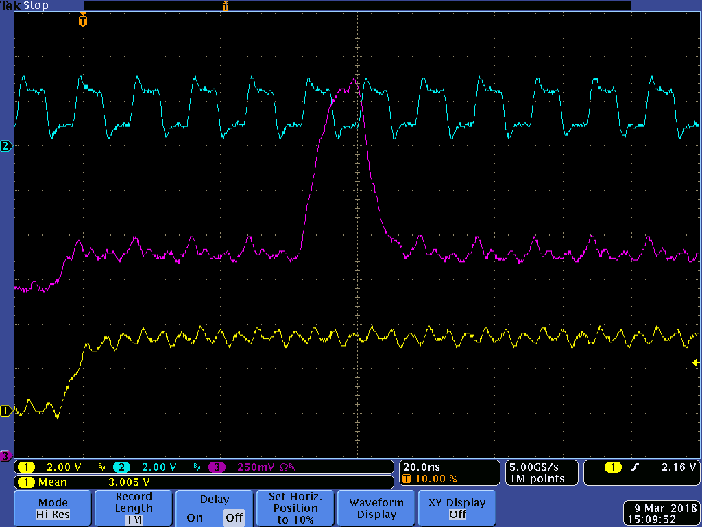
    Here is a scope plot of the signals. The blue trace is the ADC clock (taken before a clock buffer with 2.2ns delay and no inversion). The red trace is the analog (differential) input.

    The output of the ADC is used to generate an image where 4 outputs are multiplexed. Next picture is the profile of the image where pixels 3, 7, 11, 15, ... come from the analog signal seen on the scope plot above.

    The peak in the signal could be seen in the pixels 7 and 11, which are adjacent samples. This seems to correspond to latching the analog signal on the rising edge of the ADC clock.

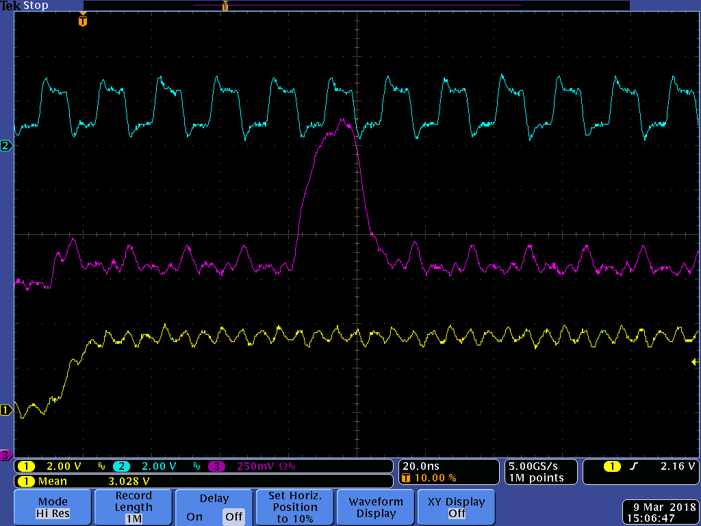
    We repeated the experiment with the same analog signal but an inverted ADC clock (shifted 180deg.) and come to the same conclusion. See plots below.

  • Vincent,

    When looking at your plots, to me it appears the signal level is the same both during the rising edge and falling edge of the clock. Can you run with a slower clock so that the pulse is only high during one of the edges? To me, this would definitely tell which edge is being used. What is this 2.2ns delay you mention?

    Regards,

    Jim 

  • Jim,

    If you observe the first scope plot and look to the peak in the analog signal (bump in the purple trace at the middle of the plot) you would have 2 samples in the peak zone by sampling on the rising edge of the clock (blue trace), but only 1 sample if sampling is on the falling edge. We noticed 2 samples with a higher value in the ADC output ...

    The 2.2ns is the delay between the blue trace in the plot and the real ADC clock entering the ADC3443 because I probed the clock before a clock driver on our board. So the exact sampling point should be 3.6ns (2.2ns from the clock driver + 1.4ns aperture delay from the ADC) after the falling (rising?) edge of the blue trace.

    Regards,

    Vincent

  • Vincent,

    Is this still a concern for you?

    If so, is it possible to sample at lower clock rates (say 10 or 20 MSPS) such that only one sample is high.

    What pin number of the device are you monitoring for INP, INM, CLKP and CLKM? There are older copies of data sheets that had these swapped. We just want to double check this by knowing the actual pin number you are probing.

    Regards,

    Jim

  • Hi Jim,

    Yes, this is still a concern. In our application we are digitizing the analog output of an high speed image sensor where the bandwidth and settling time have been optimized to reach the expected analog value for each pixel at about 75% of the pixel period. To avoid sampling  during  transitions of other signals (e.g. from next pixel) in the camera/sensor and allow for some jitter we have to stay away from the last 10% of the pixel period. So for a pixel rate of 60Mhz we have a window of  only 2.5ns to set the sampling point.

    We have another issue in this regard: The datasheet is very spare with information about the input sampling circuit. It does't allow us to fine tune or simulate the driving circuitry from our camera.  The datasheet of ADS6444, for instance, provides much more information about the analog inputs (see page 48).

    Herewith the pin functions list we used:

    CLKP - 22

    CLKM - 21

    INAP - 9

    INAM - 8

    INBP - 12

    INBM - 13

    INCP - 31

    INCM - 30

    INDP - 34

    INDM - 35

    Regards,

    Vincent

  • Vincent,

    Is it possible to send a narrow pulse that is centered about a rising or falling edge only? You could use a slow clock to help with this test. This should then determine with your setup if the output is sampled on either a rising or falling edge.

    Regards,

    Jim