This thread has been locked.

If you have a related question, please click the "Ask a related question" button in the top right corner. The newly created question will be automatically linked to this question.

ADS5444: clock input compatibility with lvds

Part Number: ADS5444

Hello

As i decide to capture converter data with xilinx spartan 6 family for initial tests, i wonder is it possible to clock the converter with lvds clock outputs of sp6 family?

I searched and found some contradictory information regarding the possibility of this connection and it's configuration type (termination resistors, etc.).

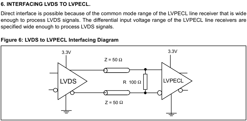
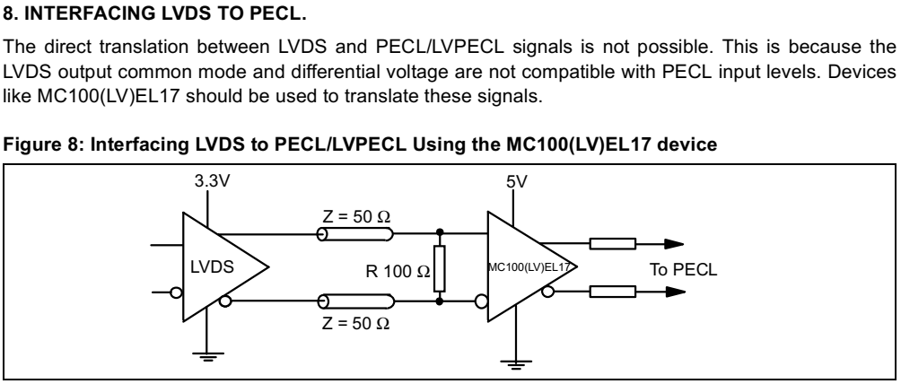
In AN1318 of STMicroelectronics titling "INTERFACING BETWEEN LVDS AND HIGH SPEED DIFFERENTIAL LOGIC FAMILIES", it is mentioned that:

these statements seem to be in contradiction.

  • Hi aseok

    It should be possible to use the LVDS outputs from the FPGA using a circuit similar to that shown in 6. above and then add a 100nF capacitor in series right at the input of each CLK and /CLK pin of the ADC. These capacitors ensure the inputs are biased at the proper input common mode for the clock receiver.

    Please note that since the amplitude of the LVDS signal will only be about 0.7Vpp the ADC performance will not be optimal (see Figures 24 and 25 of the ADS5444 datasheet). The FPGA clock source may also have more jitter than is ideal, which can also degrade performance, especially with higher frequency input signals.

    Ideally you should use a low jitter clock source with an amplitude of at least 1.5Vpp at the ADC clock inputs. The ADS5444 datasheet refers to this additional guidance regarding clocking: http://www.ti.com/general/docs/lit/getliterature.tsp?baseLiteratureNumber=SLYT075

    I hope this is helpful.

    Best regards,

    Jim B