This thread has been locked.

If you have a related question, please click the "Ask a related question" button in the top right corner. The newly created question will be automatically linked to this question.

ADS1246: Problems running new board

Part Number: ADS1246
Other Parts Discussed in Thread: REF5025, REG1117, LM1117

Good day!

I've been developed the new board including three ADS1246. During tests I am exeriensing weird case:

1. Then issuing RDATA command I receive LSB alwais reading 0.

2. Very much noice in mid byte - about 7 bits are changing.

Here is a plot of SPI comm:

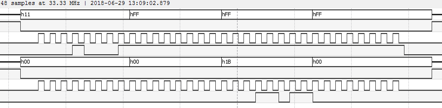
Singnals in this plot are:

[SPI decoding]

CS

CLK

SIMO

[SPI decoding]

CS

CLK

SOMI

The rest conditions are:

AINP and AINN pins are shorted with REFP pin. REFN is connected to ground. REFP in at 2.5v from REF192. Internal oscillator used. PGA is set to 8x. Data rate is set to 640SPS. START pin is high, reading occurs on DRDY signal.

What is wrong?

  • One problem is solved - wrorng comand code (11h instead of 13h) caused wrong data format.

    But it is still too noisy! 9th bit is noisy then measuring dark photodiode current!

    Also one of three ADCs outputs 7Eh in upper byte (and also in response to command byte) alwais. Could it be damaged?
  • Oleg,


    I'm glad that you were able to figure out the wrong command code.

    As for the noise problem, the noise that you see can come from a variety of sources that depend on the setup of the device and the surrounding circuitry. Are you able to share a schematic? I would need to know how you have the ADC setup and what sort of measurement that you are making.

    So far, you have said that you are using a PGA of 8 and a data rate of 640SPS. If you look at Tables 1 and 2 of the datasheet you can find some values for the expected noise performance of the device. For your settings, I would have guessed that you would get about 11uV of peak-to-peak noise. This translates to just under 16 bits of noise free performance. Additionally, you are using a REF192 which has a noise voltage of 25uVp-p (within the 0.1Hz to 10Hz bandwidth). All of this noise will be seen at the full scale (referenced to the output of the PGA). I would use a lower noise reference like the REF5025.

    If one of your ADCs is reporting something like 7Fxxxxh, this means that the input signal is reading near positive full scale. It is possible that the device is damaged, but I would look for other setup problems first. It's possible there's a problem in construction, where the input is over-ranged, either by shoring the AINP connection to positive supply, or by over-ranging the PGA. Also, you might have a bad connection to the reference. If the reference is near 0V because it is unconnected, you might have some over-range issues as well. Regardless, I would check all the connections to the device first.


    Joseph Wu

  • Attached schematic of signal input and ADC (Sorry, if file name is unreadable, it's cyrillic).

    I tried to reduce data rate to lowest value of 5SPS, but noise is not changed. Also, ADC with shorted input (AINN connected to AINP and to REFP) outputs data with 7 lowest bits of noice.

    I'll try to replace REF.

    АКЛС.020.656.000 Блок фотодатчика.PDF

  • The bogus ADC reads 7E in high byte, not 7F. Measured between AINP and AINN of this ADC is about +40mV, and when I apply light to photodiode it rizes, and low bytes reading is rizing too.
  • Oleg,


    For the one device of the three that has 7Eh as the upper byte value, it's hard for me to know what the problem is.

    It seems that you are able to get correct values from the other two devices on the board. If the devices are all connected the same way, but one is giving unusually large values, then it's unlikely the device that is the problem. However, there are several possibilities.

    As you suggested that device may be damaged. If you do suspect damage, I would remove the device and replace it with a new one.

    You mentioned that you measured the input to be 40mV. With a gain of 8, that makes the measurement equivalent to 0.32V. Just so I know the value, check the common mode value of the input to be sure that the input can be measured by the PGA. At least measure AINP and AINN with respect to the AVSS voltage. The input voltage must be within the common-mode input range of the PGA. This is described in the Low-Noise PGA section onf the datasheet on page 26. Having the input common-mode voltage outside the PGA range won't make signals large, but I did want to know this value to be sure.

    At the same time, you should measure the reference value. If the reference is significantly lower than expected, then the data may be high. By measuring both the input and the reference you can confirm that the device is acting like an ADC.

    Check your code to see if you have the configuration for the device incorrectly set. If you accidentally set the wrong gain, then you would get a significant error.

    After that, I would look at a problem in the board manufacturing. If inputs or the reference are incorrectly connected, or the there are bad solder connections, then you may get errant values.

    For the noise problem, I'll also need more information about your application. I'm not very familiar with photodiode applications, so I'll need to know how you have the photodiode connected, what measurements you are making, and what the voltages are for the device. It would also help to get a series of data to show the noise for 640SPS and 5SPS. This would show how different the noise performance is in different configurations and show if there is any periodic noise. It would also help to get a series of measurement values for inputs shorted as well as measurements for the photodiode dark current.

    I would check for the board for any oscillations or any ripples in the power supply. The REG1117 is recommended to have much higher input capacitors (and output capacitors if the output isn't 10uF). I'd also short L1 in case it causes some stability problems.


    Joseph Wu
  • Thank you for answer!

    Tomorrow I'll try to replace all three ADCs.

    Note, in the begining ov tests, there was a problem with REF192 - first one was damaged and outputs 4.7V. As I see in datasheet, the Differential reference input voltage should be no more than AVDD-AVSS-1, so it should not be higher than 4V, so it could damage the ADCs.

    Also I'l add more capacitors to 1117s.

  • Oleg,


    Thanks. I'll wait for your results. There were two things that I wanted to note about your last post:

    Having the reference voltage input above AVDD-AVSS-1 (or 4V with a 5V supply) may cause some bad data, but will not damage the device.

    I would also remove L1 and replace it with a short at the output of the LM1117. Inductors would normally try to keep the current constant. However, with digital circuits, the current is always switching, this can cause spikes in a supply with the Ldi/dt. In general, I avoid inductors around the ADC supply.


    Joseph Wu
  • Oleg,


    I haven't heard from you for a week and I was wondering if you had a solution to readout issues. I'll close the post for now. However, if you don't have a solution and still have readout problems, you can post back and we can continue to debug your system.


    Joseph Wu
  • Hello!

    Sorry, I was busy solving different problems.

    For now, summary is:

    1. I changed PGA gain from 8 to 1, as PGA seems to amplify internal noise. Instead, I rised trasnimpedance resistor from 100k to 820k, increasing gain of in 8 times. This lowered noise significantly.

    2. Changing REF192 to REF5025 has no effect at all.

    3. All ADCs was replaced, and reading is the same now.

    4. Noise is very high anyway, about 9-10 bits. Shorted input provide noise at about 7 bits.

    5. Strange, but noise is not reduced, if I change SPS to lowest values.

    6. Synchronized conversion using START pulse before each conversion provide extremly noisy results, so I use continuous conversion mode, START is high alwais.

  • Oleg,


    In one of my previous posts, I went through several things that you could check. It would help to let me know what it is that you went through to verify some of the things that I mentioned.

    Also, it would help to know the configuration of the ADC is when you make measurements. This would be for both gain, data rate, and input voltage. Here, I'm assuming that you're using a 2.5V reference. Then, when you report back the output, I'd need to know the output code, and noise statistics (mean, standard deviation, etc in code) it helps with the analysis. I would want to relate those values back to the input voltage seen by the ADC.

    Additionally, you might want to compare the noise when you have the inputs shorted to the noise tables shown in the datasheet. This might also help with the analysis.

    One other thing, as I mentioned in a previous post, I'm not very familiar with measurements using a transimpedance amplifier, and a photodiode. However, it seems to me from the schematic you provided that the feedback resistor is a bit large, and the feedback capacitance is very large. Have you tried removing the feedback capacitance or replacing it with something under 10pF?


    Joseph Wu