This thread has been locked.

If you have a related question, please click the "Ask a related question" button in the top right corner. The newly created question will be automatically linked to this question.

ADS7841: Allowable source impedance

Part Number: ADS7841

Hello,

I would like you to confirm about below.

* Could you please tell us allowable source(input) impedance ?

We would like to input voltage which is devided by resistor to CHx.

However, there is no spec about source impedance. So, we are not sure how many resistor value should be allowable.

Best Regards,

  • Ryuuichi,

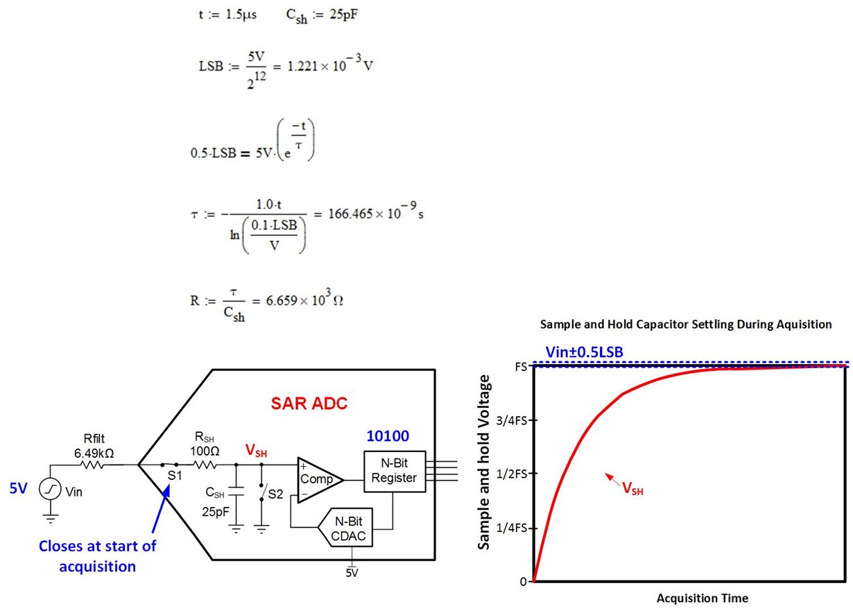
    The input to this device is a switched capacitor input. So the input impedance is actually a dynamic impedance (i.e. it changes as the input capacitor charges up).  Each time the ADC converts analog to digital the internal sample and hold capacitor Csh will be charged up.  To get an accurate conversion result the capacitor needs to be charged to ½ of an LSB.  If the capacitor is not sufficiently charged up it will appear as though the input voltage is really lower than it actually is.  Once the capacitor is fully charged up, the input impedance of the SAR is very high.  So, the size of impedance that can be connected to the input of the ADC depends on the internal capacitance and charge time allowed.  The info below shows how to calculate this maximum impedance.

    The switch S1 is closed for each conversion during the acquisition phase. The minimum acquisition time for this converter is 1.5us (for a 200ksps sampling rate).  For slower sampling rates the acquisition time will be longer.  For the purposes of your question I will assume that you are sampling at 200ksps.

    So, the answer to your question is that the largest source impedance needs to be small enough to allow the sample and hold capacitor Csh (25pF from data sheet) to fully charge up during the 1.5us acquisition period. In this case solving the RC charge equation shows that a 6.6k ohm resistor could be used to fully charge during the 1.5us acquisition phase.  Below is the math and example circuit.  Keep in mind that if you use an amplifier to drive the input, you may be able to achieve better results using an RC filter on the front end.  I suggest you review TI Precision Labs on SAR ADC Front End Component Selection video series for more details.


  • Hello Art-san,

    Thank you for your detailed explanation.

    I have one question about above. (Maybe this is mistake of quote.)

    * The minimum acquisition time for this converter is 1.5us (for a 200ksps sampling rate).

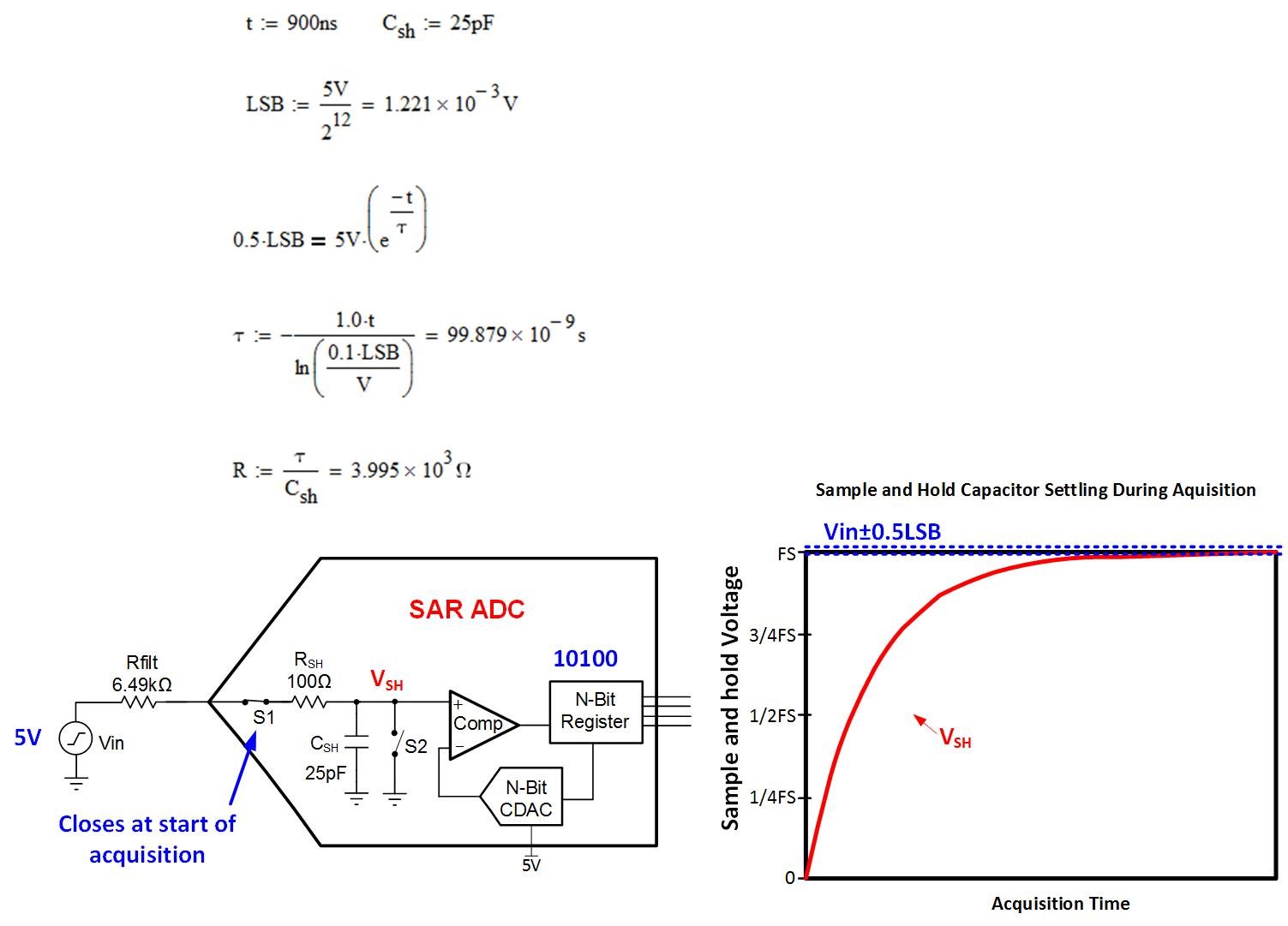
    You described above, but I think when full scale is 5V, 900ns is minimum acquisition time.

    Because, 1.5us is acquisition time when Vcc = 2.7V to 3.6V.

    Is it just mistake of quote ?

    Best Regards,


  • You are correct. I looked at the wrong table.  The updated answer is below.  The same method applies.


  • Hello Art-san,

    Thank you for revising.

    I also noticed that you should change formula as shown below.

    *0.5 LSB = 5V [ e^(-t/τ)]

    =>

    Vin-0.5LSB = 5V - 5V [ e^(-t/τ)]

    The formula which you indicated is for falling edge.

    In case of rising edge as shown above, formula should be V = FS * (1-[ e^(-t/τ)]).

    Could you please confirm ?

    Best Regards,

  • Hello Art-san,

    Could you please send me your feedback ?

    If my understanding is NOT correct, please correct me.

    Best Regards

  • Ryuuichi-san,

    Vin=5V so my equation is equal to your equation.  Subtract 5V from both sides, and negate both sides.  Let me know if this is clear.  I believe that both equations are equivalent.


    0.5 LSB = 5V [ e^(-t/τ)] (my equation)

    Vin-0.5LSB = 5V - 5V [ e^(-t/τ)]  (your equation)

  • Hello Art-san,

    Thank you for your reply.
    In above case (VIN = Vref), I understood that we can get same result.
    However, in customer case VIN ≠ Vref, so I will use this "Vin-0.5LSB = FS- FS [ e^(-t/τ)]" formula.

    Best Regards,