This thread has been locked.

If you have a related question, please click the "Ask a related question" button in the top right corner. The newly created question will be automatically linked to this question.

ADS8902B: LDO output voltage issue

Part Number: ADS8902B
Other Parts Discussed in Thread: PGA280, OPA320, OPA625

Hi...

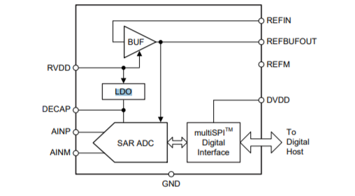
I have some problem with ADS8902B.

When I change the sampling frequency(through CONVST pin) from 10kHz to 100kHz/200kHz/250kHz, LDO output(DECAP pin) voltage is dropped(1mV to 2mV),

and the dropped voltage is different according to the sampling frequency.

I already changed and tested a decoupling capacitor from 10uF to 1uF(X7R), but the result was the same.

Could you recommend the solution for this problem?

Please let me know that.

ADS8902B_Schematic.pdf

Regards,

Jeffrey.

  • Hi Jeffrey,

    In ADS8902B, the internal LDO is used to power the ADC core.

    When you change the sampling rate of the ADC from 10-kHz to 250-kHz, the current drawn by the ADC core increases.
    This increased current can result in change in LDO voltage (load regulation). This minor variation in LDO voltage will not impact device performance
    It is OK to use 1-uF decoupling capacitor on DECAP pin.

  • Hi Rahul,

    Thanks for your comment.
    You said that this minor variation in LDO voltage will not impact device performance.
    But this minor variation impacts ADC performance of this device.
    For example, when LDO output voltage increases by 1mV, output value of this device increases by 10 proportionally.
    Also, when LDO output voltage increases by 2mV, output value of this device increases by 20 proportionally.
    When these measurement data are finished, I'll show you that.

    Regards,
    Jeffrey
  • Hi Jeffrey,

    Thanks for this additional information.

    For a given input voltage, if the output code is changing with change in sampling rate it might be due to insufficient time for charge kick-back settling on the ADC input. I reviewed the schematic snippet in your original post and the RC time constant looks OK.
    If you don't mind, could you share the schematic showing driver amplifier as well.

    You can share it with me offline via email (rahulvk@ti.com).
  • Hi Rahul,

    Please refer to the bellow schematic included the amplifier.

    PGA280_ADS8902B_Schematic.pdf

    Regards,

    Jeffrey

  • Hi Jeffrey,

    The PGA280 has relatively lower output bandwidth than what would be required for this design to operate at 250-kSPS. When using the ADS8902B at 250-kSPS, the settling time available to the amplifier would be 4µs - conversion time (1.2µs) = 2.8µs.

    Referring to the settling time specs in PGA280 datasheet, the PGA280 will not support this sampling rate -

    If it is required to operate the ADS8902B at full speed, you could consider using a buffer amplifier, such as OPA320, at the output of the PGA280.

    Please refer to this TI Precision Lab video for more details on this topic.

  • Hi Rahul,

    Thanks for your comment.

    ADS8902B has the delay time of almost 1ms because PGA280 has the long settling time of 30us at G=8, Vo=8Vpp.

    So I think that the settling time of ADS8902B is enough.

    I have measured the raw data(2048 samples) of ADS8902B output by each sampling frequency. (10kHz/30kHz/60kHz/120kHz/150kHz/180kHz/210kHz/240kHz)

    But the calculated voltage values are so different, and the gap is from 1mV to 32mV.

    Could you explain in it?

    Measurement data.pdf

    Regards,

    Jeffrey

  • Hi Jeffrey,

    Rahul asked me to take a look at this.

    I do think at least part of the problem is with the PGA280; too slow settling on the output stage to support 20b at higher sampling rates. However, there may be something else contributing to these errors.

    Can you answer the following questions?

    1. What voltage is the reference input, ADC_REF?
    2. What voltage is the output common mode of the PGA280, VO_CM.
    3. Can you confirm that the bypass capacitors are all ceramic, including C85 on the REFOUT pin of the ADS8902B?
    4. Can you confirm the input filter caps, C82/C83, are ceramic C0G/NPO type?
    5. Also, for the attached measurement data, I see a code count of ~4600. Is the ~1800mV (I assume this is microvolt) at the input of the PGA280, and what is the gain setting of the PGA280 for these measurements?

    Thank you,

    Keith N.
    Precision ADC Applications
  • Hi Keith,

    Thanks for your feedback.

    Please refer to the bellow answers.
    1. What voltage is the reference input, ADC_REF?
    : 4.096V
    2. What voltage is the output common mode of the PGA280, VO_CM.
    : 2.048V(=4.096V/2)
    3. Can you confirm that the bypass capacitors are all ceramic, including C85 on the REFOUT pin of the ADS8902B?
    : All X7R or X5R grade ceramic capacitors
    4. Can you confirm the input filter caps, C82/C83, are ceramic C0G/NPO type?
    : X7R grade ceramic capacitor
    5. Also, for the attached measurement data, I see a code count of ~4600. Is the ~1800mV (I assume this is microvolt) at the input of the PGA280, and what is the gain setting of the PGA280 for these measurements?
    : 1799mV, and gain setting 1/4(=0.25) V/V

    Regards,
    Jeffrey
  • Hi Keith,

    We have done some tests to reslove this problem.
    We have changed the capacitors only of charge-kickback filter from 10nF to open, and then this issue has been improved almost.
    We think that this test result can be the solution for this problem.
    We want to know the recommended value range of charge-kickback filter. (capacitor and resistor)
    Also, when the capacitor value of charge-kickback filter is changed from 10nF to open, how to select the resistor value?

    Regards,
    Jeffrey
  • Hi Jeffrey,

    I agree that all data points to the PGA280/charge bucket filter. I am sure there is room for optimization, but I still doubt you can get to full performance of the ADS8902B when using the PGA280 alone at higher sampling rates.

    In order to optimize the charge bucket, I will need to see if we have a spice model available. As mentioned earlier, the only way I know to guarantee performance is to add a higher speed buffer, such as OPA625, which was used on the evaluation board.

    Please give me a few days to investigate.

    Thank you,
    Keith N.
  • Hi Keith,

    Thanks for your comment.
    Unfortunately, we can not add a high speed buffer because the board was fixed, and the development is being finished almost.
    So we should find the solution to reslove or improve this problem.
    We're sorry but we hope that you give us some feedback quickly.

    Regards,
    Jeffrey
  • Hi Jeffrey,

    Just a quick update; I found a model for the PGA280 that I can use to optimize the charge bucket filter. This should predict the best performance that you can get in this configuration.

    I will provide an update no later than end of business tomorrow.

    Thank you,
    Keith N.
  • Hello Jeffrey,

    Based upon several simulation runs,  the best RC combination for the charge bucket filter is 6.04ohm and 1.2nF differential, or 6.04ohm and 2.4nF single as shown below.  According to the results, 100ksps is the best sample rate you can achieve and get settling in the 20b range.  At 250ksps, you can expect 18b of performance with this filter combination.

    Thank you,

    Keith N.

  • Hi Keith,

    Thanks for your simulation result.
    We'll test your simulated filter combination, and then let you know our test result.

    Regards,
    Jeffrey
  • Hi Keith,

    We have tested your simulated filter combination on our board.
    But there was a little improvement effect on output code variation.
    For example,
    When your filter has applied on that, there is about +/-15uA output variation at 1800uA input condition by each sampling frequency.
    Otherwise, our filter(resistor=0ohm, capacitor=open) has applied on that, there is about +/-3uA output variation.
    Is there any side effect or expected problem about this combination(resistor=0ohm, capacitor=open)?

    Regards,
    Jeffrey
  • Hi Jeffrey,

    The PGA280 can be directly connected to the ADC inputs without a charge bucket filter, but I do not have any data or models to predict how well this will work over a large number of devices and operating conditions. If this is the direction that you want to go, I suggest verifying system performance with multiple devices over temperature, and at multiple sample rates.

    Thanks,
    Keith N.
  • Hi Keith,

    Thanks for your comment.
    We'll verify the system performance with multiple devices at multiple sample rates.

    Regards,
    Jeffrey