This thread has been locked.

If you have a related question, please click the "Ask a related question" button in the top right corner. The newly created question will be automatically linked to this question.

ADS8885: What are these input driver symbols

Part Number: ADS8885
Other Parts Discussed in Thread: OPA333, ADS8695, ADS1115, OPA191, ADS8691, TINA-TI, REF6030, OPA320

Hi,

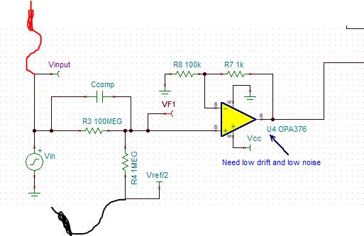
I am a beginner when it comes to DAQ, I am trying to learn but I keep coming upon some symbols that I don't understand.
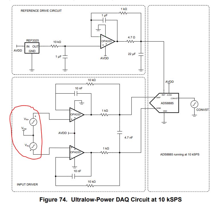
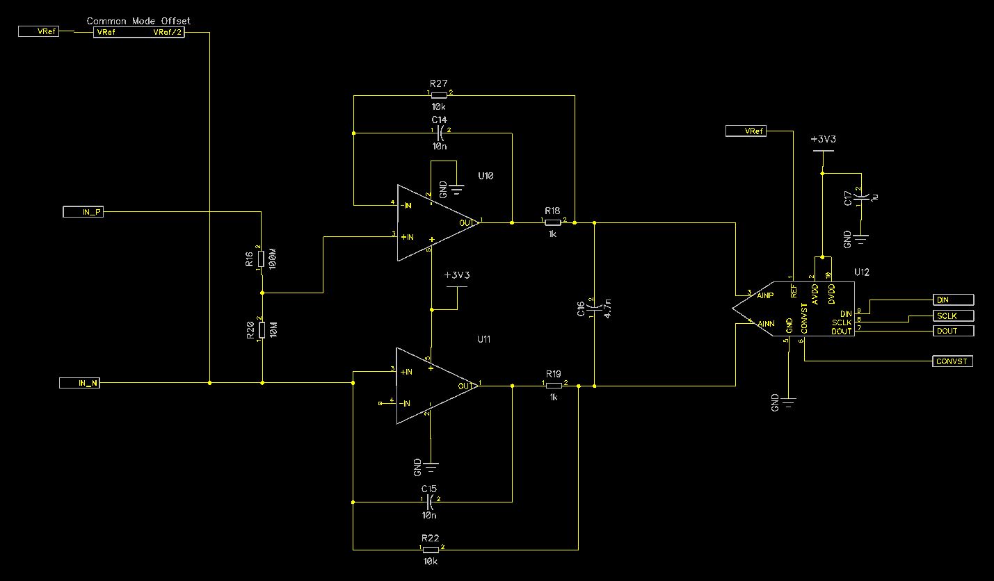
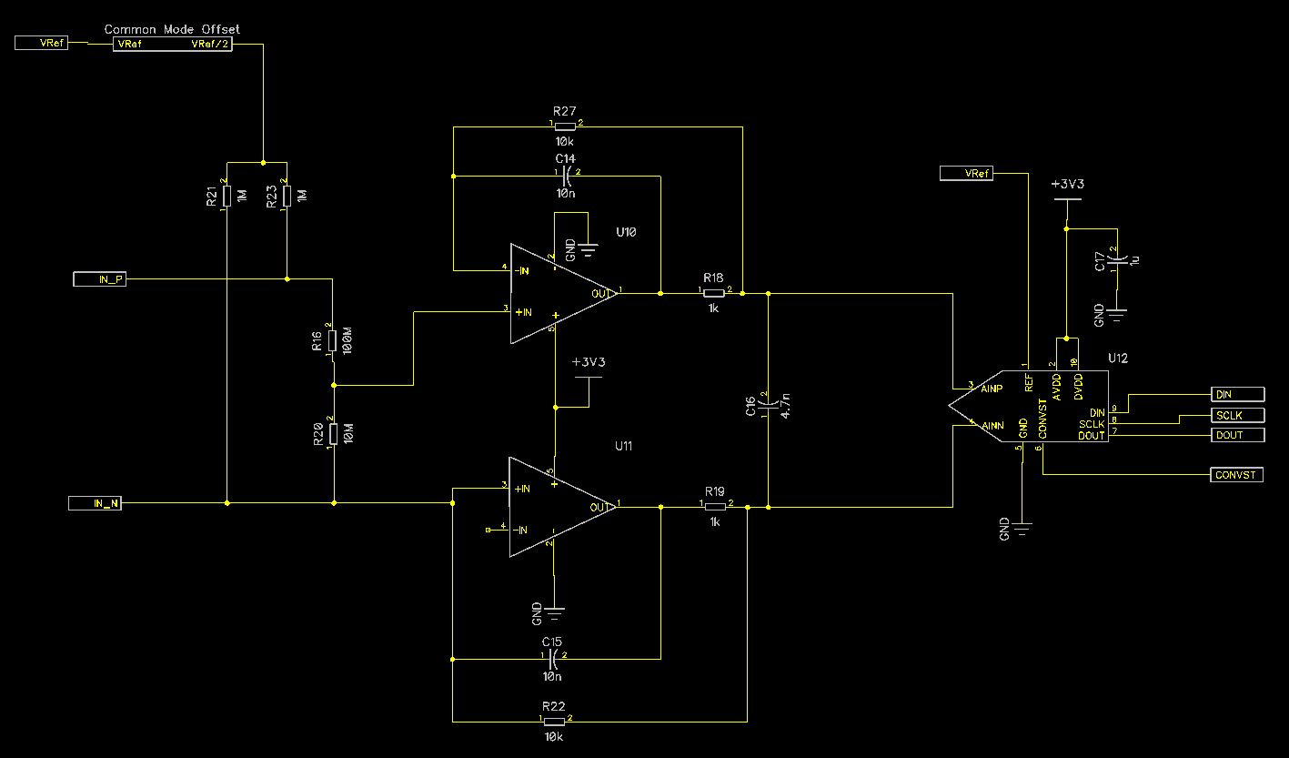
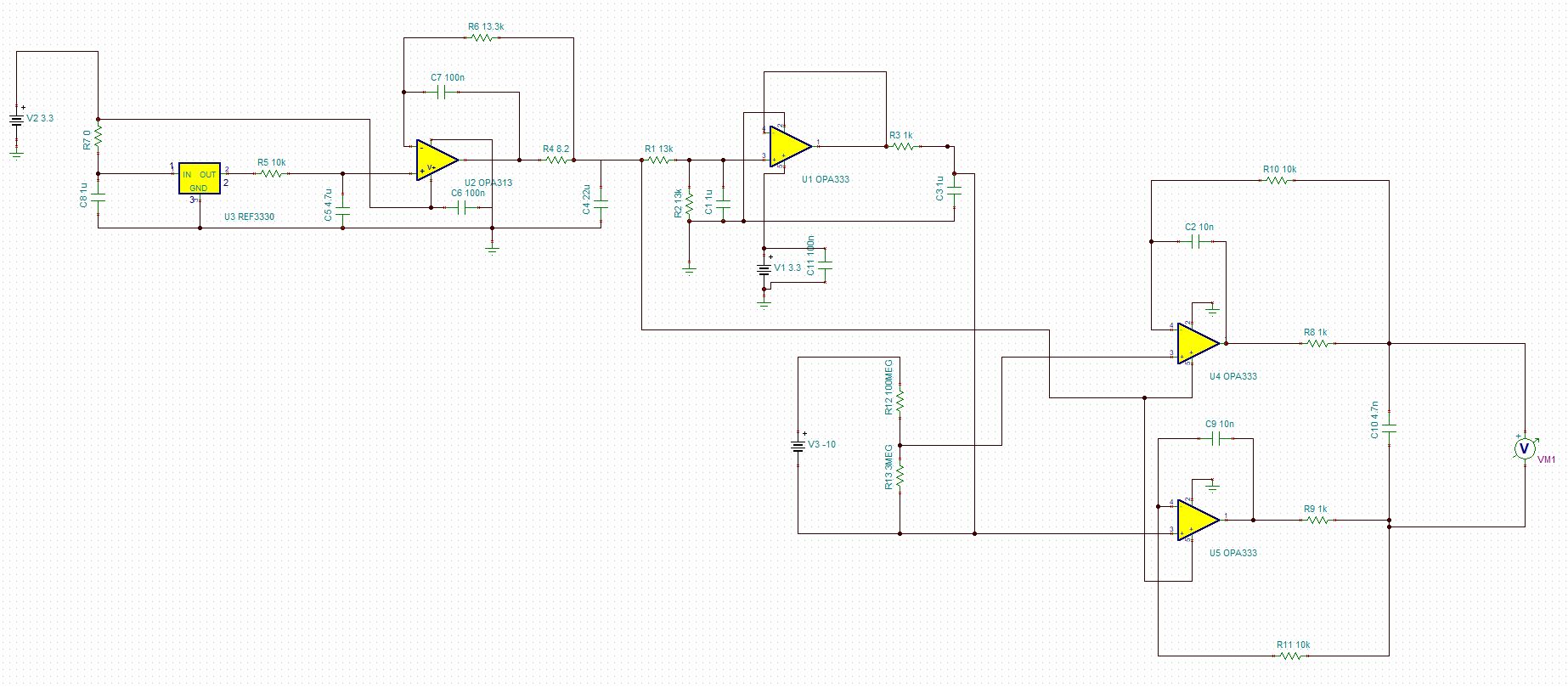
I dont know what the "Step inside a circle" symbols is here. Nor do I understand the function of this part of the circuit.

The best that I can guess is that they are trying to show some kind of common mode offset, maybe Vref/2?
If so, can this be done with just a pair of resistors in a divider? Is this sufficient or is there a much better way?
I cant quite get my head around this could someone be so kind as to show me what this circuit looks like in real life?

Thanks


  • Hi Sam,

    These symbols represent a generic voltage source. For a steady DC value, a battery symbol could be used, but these represent any input voltage source including DC and time varying input voltages such as a step input, a square wave, sine wave, etc. For example, a function generator can be represented by this symbol.

    This specific configuration is showing how a differential input voltage would look. Vin+ and Vin- are equal in magnitude, but opposite in phase. Vcm represents a fixed, DC level, that is typically 1/2 of the reference level used for the ADC.

    Regarding your question on Vcm, it is typically generated with a resistor divider from Vref, but depending on the input circuit configuration, usually requires a buffer amplifier. Most Differential input ADC's require a specific common mode voltage level on the inputs, but the ADS8885 is much more flexible. Each of the two ADC inputs, AINP and AINN, can be any voltage between -0.1V and Vref+0.1V. In Figure 74 above, the reference in this circuit is 2.5V, so the ADC inputs can accept voltages between -0.1V and 2.6V, and still provide an accurate conversion result of AINP-AINN.

    If you are new to using high precision ADC's, I highly recommend you view TI Precision Labs - ADCs and TI Precision Labs - Op Amps. There are excellent tutorials for both beginner and experienced engineers alike. There will explain all of the different input structures and required drivers for the different types of ADCs on the market.

    training.ti.com/ti-precision-labs-overview
    training.ti.com/ti-precision-labs-adcs
    training.ti.com/ti-precision-labs-op-amps

    Thank you,

    Keith N.
    Precision ADC Applications
  • Thank you very much Keith, for your helpful answer and for pointing me in the right direction for more help.

    I have been going through these labs this morning and I am learning quickly. Though I think I still have a gap that maybe you can help resolve.

    My understanding is that the ADS8885 is a True Differential ADC. Does that mean that you don't have to offset the input at all?

    Does the above circuit depict a Pseudo Differential Circuit rather than True Differential?

    I see that the Operating Input Range for both AINP and AINN is -0.1V to Vref+0.1V.   I assume that this is with respect to the ADC GND. I am designing a battery powered portable instrument, this is floating with respect to what the measurement measures, does that mean that to measure a true differential signal I have to tie my supply GND to one of the measuring terminals? i.e does that mean that it is not possible to make a true differential measurement with a battery powered device? Or conversely, is the fact that the instrument is battery powered make it easier to make truly differential measurements because it is isolated from ground?  

    Finally I came across a TI design that uses an OPA333 to divide VReff/2 to create a Vcm I plan to use this type of circuit rather than just a resistor divider. I get stuck at the point of connecting it to InP and InN. my understanding is that if I connect it to just InN then I will be making a Pseudo Differential Measurement, but if I connect it to InN and InP then InN=InP=VReff/2 (WRT GND)   therefore VDiff = 0. Obviously, I am missing something very fundamental

    Here are my 2 ideas, the first I think makes a Pseudo Differential measurement, the second I believe will have measurement errors introduced by R21 and R23.

    Am I wrong on either/both accounts?

  • Hi Sam,

    Answers to above questions.

    1. With the true differential input, you can ground the AINN input. However, you will now only be able to measure 'positive' differential voltages which reduces the resolution of the ADC by 1b, you are losing all of the codes that represent a negative differential input.
    2. The above circuit represents a fully differential input, meaning that both the AINP and AINN inputs can move within the -0.1V to Vref+0.1V range. For a pseudo-diff input, the AINN is fixed at a DC level, usually 1/2 of the Vref.
    3. The reason to do a differential measurement is to reject a common mode voltage relative to the measurement circuit ground. If the measurement circuit power ground is completely isolated from the source, then you do not need a differential measurement.
    4. Based upon your above circuit, it looks like you are trying to measure an input voltage attenuated by a voltage divider. (I assume your input voltage is always positive relative to ground.) In this case, I would configure the input similar to a pseudo-diff input. Generate Vref/2, buffer it and feed it into the AINN input through the charge bucket filter. Connect your input resistor divider ground (low side) to the measurement circuit ground, and simply measure the single ended input.

    Take a look at the ADS8695. This part is a similar 18b device, but includes the front-end driver amplifier and a programmable PGA, that will allow the measurement of bipolar or unipolar input signals.

    Regards,
    Keith N.
  • Thanks again Keith,
    Could you comment on which of the two schematics that I posted is the correct way to wire "Fig 74" (from the original post) if either?

    The differential voltage that I am measuring could be positive or negative and I have no Idea what it is relative to ground as the instrument it is battery powered. Is this something that I should know?

    I will take a look at the ADS8695, the instrument that I am making needs an input impedance of at least 100M, hence the largish R divider. I can't have anything of relatively low impedance in parallel to the input. I made a previous version of this instrument with 200M impedance using an Instrumentation amp, then an ADS1115 but I need to significantly increase the sample rate. My understanding is that the bandwidth of Instrumentation amps makes them unsuitable for driving a SAR at high frequencies.

    Regards

  • Re-reading your comment, I am completely confused by your "point 3". If the measurement is not differential, what is it? single ended? Doesnt that mean that I can only measure positive voltages?
  • OK I have re-watched the videos which describe ADC input types, and taken extensive notes. See.

    As the two OPA333s will ensure that AINP and AINM remain in the range of 0-AVDD, and as the ADS8885 is a "True Differential" ADC, does this mean that I don't need to bias the input at all? Can it be "floating"? do I lose some dynamic range if I do this?

  • Hi Sam,

    Sorry my previous comments were confusing.  I have a few high level questions, and then we can dig into specifics.

    1.  What is the input voltage range that you need to measure?  +/-10V, +/-100V, etc.?
    2.  What is the maximum data rate that you would like to achieve?  Figure 74 of the datasheet was optimized for low power and is only good for 10ksps.
    3.  What kind of resolution, or dynamic range, do you want to achieve?  Is 18b the minimum?

    Also, using a 100Meg-10Meg input divider will result in very low signal bandwidth.   This impedance will interact with parasitic board capacitance and limit you to at most 10kHz of bandwidth.

    The ADS869x family that I mentioned before has a 1Meg input resistance.  In order to achieve 100M, you would need an input buffer.  OPA191, for example, can be powered from +/-15V supplies, and drive the input of the ADS8691.

    Regards,

    Keith N.

  • Thanks Keith,

    I would like to be able to measure +/-50V I need to measure AC and DC (calculating AC in software)  I think that 10kHz will be sufficient, though if I could easily get up to 200kHz I would take it. The 100M input impedance is critical (potentially I could go as low as 50M but there would have to be a good reason)

    I would like to get 18bits of resolution. the previous version of this instrument only used a 16bit ADC but to compensate I made it dual range, +/-5V and +/-50V (both with 200Mohm input impedance) (I was only sampling at ~650Hz). 18bits would mean that I can get away with a single range. 

    The device is battery powered from 3 AAAs. Ideally, I would like to be able to use rechargeable batteries meaning that supply voltage could be as low as 3.6V. I want to avoid switching in the power supply (for both noise and cost) so planning to use an LDO, (TPS78233)

    This is why I am looking at single supply ICs and trying to learn how to bias properly. 

    I downloaded TINA and have been able to do some experimenting/learning.

    I learned that:

    I can bias both AIN_N and AIN_P by connecting both to Vcm via resistors but they would have to be high (say 500M) and fairly well matched. This seems to have the benefit of removing Zero offset, but the practicality/expense of the resistors might be prohibitive.

    I can connect Vcm to just AIN_N. I get a Zero offset but I can calibrate/compensate in software so it is no big deal. The output is very linear for DC inputs. Below is my test circuit

    Note:
    I haven't tested with an AC inputs yet,
    The circuit is mostly a combination of the "10kHz Low power" reference circuit that was in the original post, and a TI Wireless DMM showcase reference circuit.
    Your circuit with the ADS6891 seems a little simpler

    Regards


  • Hi Sam,

    Please see example signal chain; 100MEG input resistance, +/-50V input to ADC input using 3V reference.  The entire signal chain can be powered from a single 3.3V supply.

    Since you are using TINA-TI Spice, attached is the simulation file.

    A few comments on your above circuit.

    1.  I see you are using the example circuit for the reference buffer in the datasheet.  I suggest you move to the REF6030, which is a newer device and integrates the high speed buffer.  This part eliminates the 2-opamp compound buffer circuit.

    2.  You have Vin- to the ADS8885 biased at a fixed Vref/2.  This will certainly work, but you are losing 1b of resolution, since the maximum input that the ADC will now see is +/- Vref/2.  In order to get a full 18b, you need to drive it in a full differential mode to get the full +/-Vref range.  (The configuration that you have is a pseudo-differential drive.)

    3.  The OPA333 will not be capable of driving the ADS8885 inputs for sampling rates much greater than 10ksps.  If you want to achieve 200-400ksps, then the OPA320 will be needed.

    I hope you find this helpful.

    Regards,
    Keith N.

    ADS8885 Signal Chain with 100MEG input.TSC

  • Wow, thank you very much for your incredibly helpful and thoughtful reply.

    Unfortunately, I can't open that TINA file but I will reconstruct the circuit from the image.

    I am honestly still hazy regarding how to drive the inputs for a full differential measurement. Hopefully, after playing around with your circuit I should understand a bit better.

    Regards

  • Hi Sam,

    Here is the same file that you should be able to open with TINA-TI.

    Regards,

    Keith

    ADS8885 Signal Chain with 100MEG input V9.TSC

  • That works, I have spent the mornign trying to work out how to place components like REF6030 and OPA320 which arent in my library. I downloaded a library from TI.com but cant work out what to do with it. I tried importing components as a macro but that doesnt work. I tried copying the files and folders from the downloaded library into the TINA libary but the doesn work. I found you tube video wich talks about using a libary editor tool but it doenst seem that this tool exists (maybe the video is from an older version of TINA) do you know where I can find instruction on how to import the downloaded libary to TINA?

    Thanks again for the great level of help that you have provided.
  •  Keith, finally, at the risk of asking a stupidly obvious question but not wanting to make a costly mistake. does the negative test lead get connected as shown?

  • Hi Sam,

    Regarding parts and TINA-TI, there is literature online, I think, that shows how to import libraries. However, I find it MUCH easier to go to the product folder page for a part like REF6030, and open the TINA-TI reference design. You can then just use the copy/paste inside of TINA to copy the component into your own schematic and simulate.

    Regarding the above question, the negative test lead for your instrument is the ground of the measurement circuit, not Vref/2. Vin represents the external voltage that you want to measure, and it connects to one side of the 100MEG input resistor (Positive input) and the other side connects to the measurement circuit ground (Negative input). The Vref/2 biases the attenuated input voltage up so that the single supply amplifiers always see a positive voltage (relative to their ground) for positive and negative input voltages.

    Thanks,
    Keith N.
  • Haha, of course, I was just trying to identify the voltage divider/attenuator circuit. I might be a little more confused than when I started. However, although I don't understand the circuit, it does seem to work fine, so I will have a good play with it and try to answer my own silly questions.
    I really appreciate your help and patience with this thread.