This thread has been locked.

If you have a related question, please click the "Ask a related question" button in the top right corner. The newly created question will be automatically linked to this question.

ADS7945: ADS7945: PCB layout confusions concerning connection of spilt ground (analog ground and digital ground) for GND pin (pin 1)

Part Number: ADS7945

Hi support team,

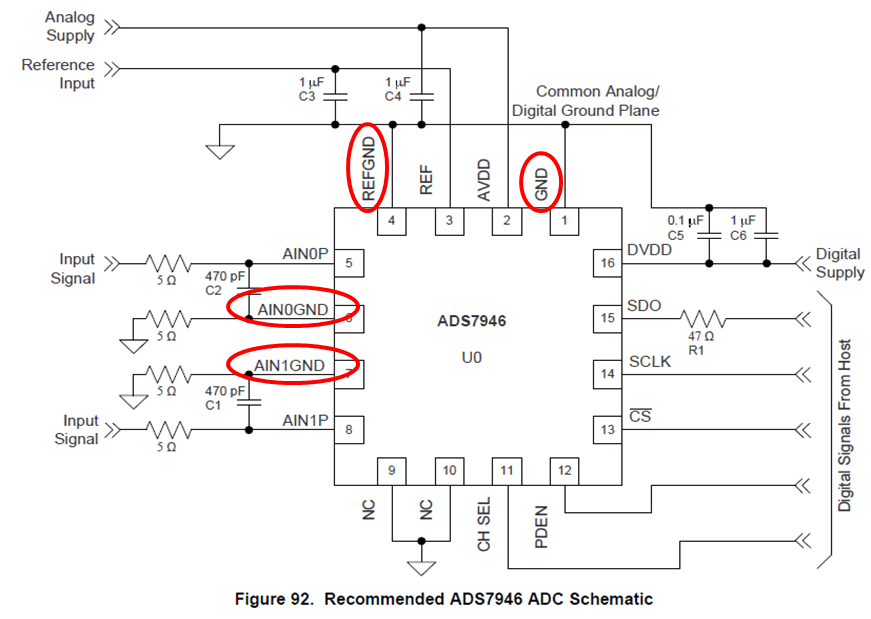
I have a question regarding PCB layout of ADS7945. It is recommended in the datasheet of ADS7945 that a spilt ground plane for analog and digital enables better results.

And the ADS7945 ground pins are connected to a common ground plane through multiple vias, which are formed by shorting analog ground and digital ground together. Since there are many ADCs used in the overall design,

a common ground plane for each ADC seems to contradict the principle of  single-point grounding in PCB layout. Hence, how do multiple common ground planes return back to power supply without any

possible crosstalk between analog ground and digital ground? What is the usual practice of PCB layout for GND pin of ADS7945? What is the relationship between common ground plane and negative point of power supply?

Sincerely,
H.C

  • Hello HC,

    Welcome to E2E forum.

    ADS7945 only has GND (pin1), REFGND (pin 4), AINx_GND (pin 6and 7), what the datasheet recommends is using a solid common ground plane, GND and REFGND can be directly connected to common ground plane on second layer by vias. The guideline is same for multi ADCs on one same pcb board, a same common ground plane is recommended. Please refer to pcb layout recommendation in Figure 91/93 and schematic in Figure 90/92.

    Thanks.

    Best regards

    Dale