This thread has been locked.

If you have a related question, please click the "Ask a related question" button in the top right corner. The newly created question will be automatically linked to this question.

ADS114S08: ADC input ripple voltage

Part Number: ADS114S08
Other Parts Discussed in Thread: LMC6082

Hi,

I using ADS114S08 part in our project to use RDT sensor interface.

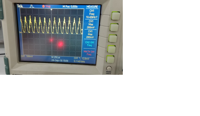
I have used op-amp buffer before to the ADC input. When i probe the ADC input signal observed more on the riiple voltage at frequency 10.5KHz range. 

I have isolated ADC input pin and verified op-amp output is very stable and clean DC voltage. When we connect ADC input pin found that the ripple is accrued.

Note : The AVDD and DVDD are no noise and clean DC voltage.

My question is :

1. Why it is ripple voltage observed when connect ADC input pin 

2. How we can remove the ripple voltage

3. What is the calculation method can be used 

Attached ADC ripple voltage waveform your reference. 

Arumugam.P

+91-9944144648

  • Hi Arumugam,

    Welcome to the E2E forum!  A few things would be helpful to know.  Can you tell me the voltages being used?  Do you have a schematic you can share?  Can you tell me the register configurations for the ADS114S08?  How are you exciting the RTD?  And how many wires (2-, 3-, 4-wire) are connected to the RTD, and the type of RTD being used (such as PT100)?  It is also not clear from the scope shot what the output of the amplifier should be or how the connection is made to the ADC inputs.

    If the amplifier is connected directly to the ADC it is quite possible that the input path contains enough capacitance to start an oscillation.  You could try adding some series resistance from the amplifier to the ADC input to see if this removes the oscillation.  There should be some series resistance added anyway as explained below.

    You shouldn't need to use an external amplifier as this will often add additional error including noise.  The ADS114S08 already includes a PGA that can be used instead of the external amplifier.  There is a guide written by one of my colleagues called A Basic Guide to RTD Measurements that is helpful in showing and calculating the RTD measurement in various application scenarios.

    The above guide explains the use of a ratiometric measurement to reduce the effects of noise and drift of the excitation source and measurement.  The ADC inputs should also include some sort of analog input filtering.  This can be done with a simple RC filter.  The analog filter is discussed in the ADS114S08 datasheet in section 10.1.2 starting on page 85.

    Best regards,

    Bob B  

  • Hi, 

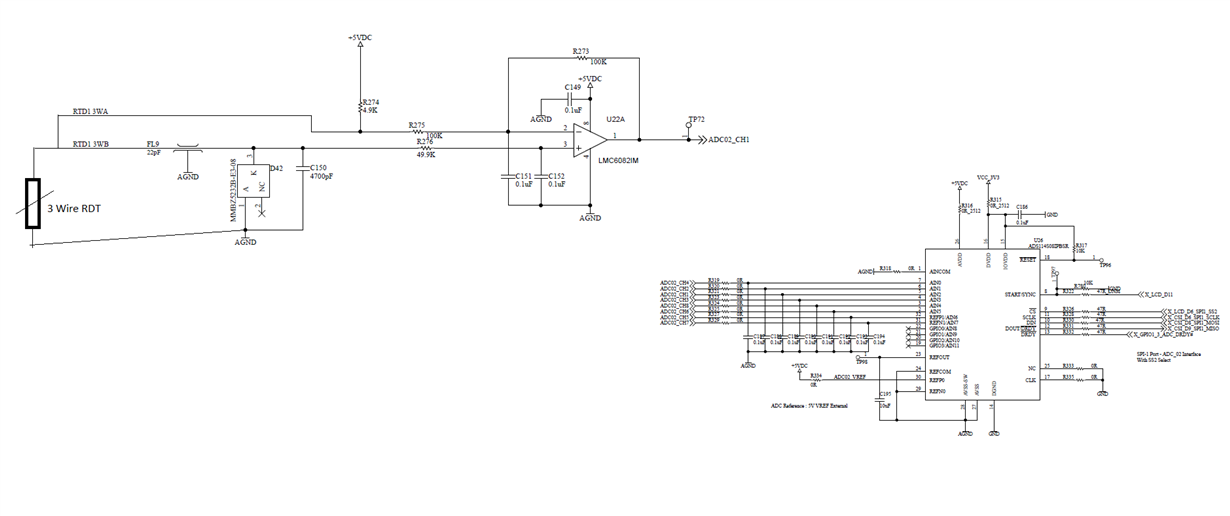
    Thanks for your reply..Please find attached schematics which answering all your question.

    3W RDT sensor PT100 used and the output waveform captured at op-amp output test point (TP72). 

    Can you please help out to removed the noise and method of calculation and calculated the R and C value to remove the noise.

    thanks in advance..

    Thanks and Regards,

    Arumugam.P

  • Hi Arumugam,

    The oscillation is created from op amp instability with large cap loading. See the LMC6082 datasheet on page 10 where it discusses CAPACITIVE LOAD TOLERANCE.

    As your input filter resistors (R319-R329) are 0 Ohm, the op amp is directly connected to a large cap load. Change these resistors to something like 1k Ohm.

    Best regards,
    Bob B