This thread has been locked.

If you have a related question, please click the "Ask a related question" button in the top right corner. The newly created question will be automatically linked to this question.

DAC8551: Serial interface specification of DAC8551 and DAC8560

Genius 15750 points
Part Number: DAC8551
Other Parts Discussed in Thread: DAC8560,

Hello,


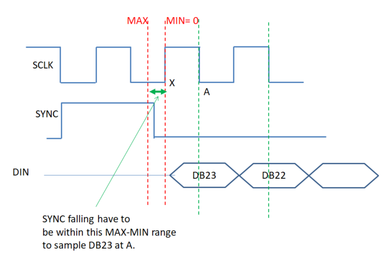
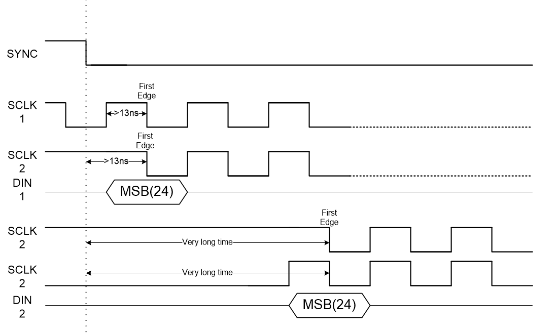
Let me just confirm a serial interface specification of DAC8551 and DAC8560.

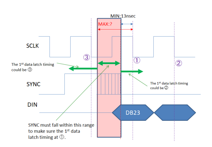
/SYNC falling edge to SCLK rising edge is defined as 0ns(MIN) in the datasheet.

But the MAX value is not available.


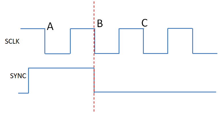
If /SYNC falls at SCLK falling edge like the below figure, which timing is DIN first sampled at, A, B or C?

Regards,

Oba

  • Oba,

    The datasheet does not provide a maximum for this specification because there is no maximum rating for this specification. The minimum simply states that the SCLK can rise at the same time as a SYNC falling edge without corruption.

    The datasheet does not provide guidance on SYNC falling edge to SCLK falling edge, therefore I would recommend avoiding the situation you have described. However, I would suspect C would be the first data latched.
  • Hi,


    Thanks for your answer.

    I understand /SYNC falling edge to SCLK falling edge case. It’s not recommended.


    But I still think MAX is required for /SYNC to SCLK rising edge timing.

    Because actually it is almost impossible to fall /SYNC at exactly the same timing as SCLK rising timing, meaning completely 0 time delay.

    There should be some delay between them.


    And because its minimum is defined as 0, to latch DB23 at SCLK falling A point in the below figure, SYNC have to fall at the same time as or before the rising edge of SCLK(point X).

    But if SYNC falls too much before SLCK rising (point X), the first data latch timing could be changed to . It could be problem.

    So I think we need to define the timing range like the below figure. So I think MAX is absolutely required.


    Regards,

    Oba

  • Hi Oba,

    It is important to note that the DACs in question do not require an initial rising edge at all.  The device only cares about the first falling edge.  We show in the figure that the clock can even be high when the SYNC line goes low. 

    I have highlighted the behavior in red.  All that matters is that data-setup time is enforced (t5), meaning the DIN value for the bit needs to be setup before the falling edge of SCLK.

    Here is some data I collected on the DAC8560, showing the state of SCLK as low for a long time and high before the falling edge of SYNC.  Data is correctly latched in both cases.

  • Hello,


    Thanks for your reply.

    I know that this device doesn't necessarily require initial rising edge of SCLK.

    I also understand the datasheet definition for “t_4 (SYNC to SCLK rising edge setup time)=MIN 0” is quite enough if SCLK stops as the figure in you answer.

    I would like to know the case where SCLK is always running. In this case, SYNC and SCLK timing is very important because DIN latch timing could be shifted depending on both timing.

    I think the datasheet doesn’t enough define timing for SCLK always running case.


    Regards,

    Oba

  • Hi Oba,

    I understand. In this case you should apply the SCLK high-time (t2) as the minimum time after the falling edge of the SYNC line, and the falling edge of the first clock that is contained in the SYNC frame.

    Thanks,
    Paul
  • Hi Paul,


    Thanks for your reply.


    I think t2 is also not enough.

    Could you see the below figure? This is my image.

    I understand SYNC must fall 13nsec(=t2) before SCLK falling edge at 1st data latch timing (1) at least.

    But it should have some range like the below figure.

    If SYNC falls within this range, 1st data latch timing is surely (1).

    If SYNC falls after this range, 1st data latch timing could be shifted to (2).

    If SYNC falls before this range 1st data latch timing could be shifted to (3).


    I think MAX value in this figure is required to make sure 1st data latch timing.


    Regards,

    Oba

  • Hi Oba,

    I understand the figure you are showing, and you are correct about which edge would be considered the first edge that data would be latched. We have based our specification on the first falling edge of SCLK after the falling edge of SYNC being the first clock edge that the DIN is valid (DB23). If condition 2 or condition 3 occur, then our timing specification is being violated and the frame is invalid (in that DB23 is not being latched in the correct position).

    Is your concern that condition 2 or 3 may occur in your system? If that is the case then I think the architecture of the SPI master must be re-evaluated to ensure the signal is more coherent.

    Thanks,
    Paul
  • Hello,


    Condition 2 can be avoided easily because the timing B in the figure is very clear. It is 13nsec before SCLK falling edge.

    But regarding condition 3, there is no way to know it. Because there is no definition about where is A.

    We absolutely need the information of where is A in the figure, meaning MAX value or something.


    Regards,

    Oba


  • Hi Oba-san,

    From a timing perspective, there is no maximum.  Most SPI devices are left-justified, and in this device's case that means the first falling edge of SCLK should be latching the most-significant bit in the for the 24bit data register.  The first 24 falling clock edges will latch 24 bits of data.  If there is an erroneous extra clock edge that that occurs after the falling edge of SYNC that is not aligned with the user's most-significant data-bit, the value on the DIN bus will be latched.  This left justified behavior is described in the programming section of the PDS.

    We also show a '1' on the first falling edge on the timing diagram, to indicate the first edge that device will latch.  If condition 3 occurs, the timing diagram is still valid, but the '1' edge will now be the new clock edge that entered the SYNC frame from do to the condition 3.

    From a timing perspective, there is not a maximum between the falling edge of SYNC and the first falling edge of SCLK. The below I have sketched a figure, showing the minimum and maximum (lack of) of the timing, with the caveat that the first falling edge of SCLK is aligned with the first data bit.  

    So in summary, there cannot be a timing maximum, but rather a functional requirement that the desired data is aligned with the first falling edge of SCLK.  That requirement is conveyed through the description of the SPI interface, and by the denotation of the first clock edge in the timing diagram.  I can see how a case like condition 3 can occur in a customers system, but the device is not able to discern with of the falling edges the user desires to be the MSB.  Because of this we must enforce the requirement the SPI master align the SYNC edges correct.

    For my clarification - is your customer experiencing this timing issue with one of TI's MCUs? Maybe we can loop in the EP team about how to modify the firmware to ensure the extra edge is not present.

    Thanks,

    Paul

  • Hello Paul,


    So, can’t this device support SCLK always running case?


    As I have mentioned before, what I’m asking is the case that SCLK is always running.

    I know that SPI peripheral in MCUs generally run SCLK only during sending the data.

    In this case, SYNC falls first and SCLK is output next. In this case, 13nsec min is quite enough specification as you explained.

    Because SCLK is not output before SYNC falling.


    But in my case, the host is not actually MCU, but is ASIC (or FPGA).

    I don’t know the exact reason but SCLK is always running even if there is no sending data.

    SYNC is only signal to start SPI communication. So SYNC have to fall within a certain SCLK timing range.

    “MAX” may not be good word, but what I’m asking is this range. There is no definition of this range in the datasheet.


    If you want to say that this device can’t support always SCLK case, please just answer it.

    I’ll discuss how to solve it with the customer. I just asked because from the datasheet timing figure, it looks to support SCLK always running case.


    Regards,

    Oba

  • Hi Oba,

    This device has no issues with a continuous SCLK.  The customer must only ensure that the most significant bit on the DIN is set-up before the first falling edge of SCLK after the falling edge of SYNC.

    Below I have drawn 3 valid cases showing the where the falling SCLK edge can occur after the SYNC Falling Edge. 

  • Hello Paul,

    Thank you very much.
    I fully understand it now.

    Regards,
    Oba