This thread has been locked.

If you have a related question, please click the "Ask a related question" button in the top right corner. The newly created question will be automatically linked to this question.

ADC16DV160: clock driven from FPGA

Part Number: ADC16DV160
Other Parts Discussed in Thread: DAC5682Z, LMK04828, CDCM7005, LMK04803, LMK04133, LMK03806, CDCM6208

Hi

I am working on a university project, developing a board containing both the ADC16dv160 and DAC5682Z, both connected to an FPGA.

I need help with the clock configuration.

If it is possible I would like not to use a clock generator but drive it directly from the FPGA (LVDS signals). Alternatly a simple one.

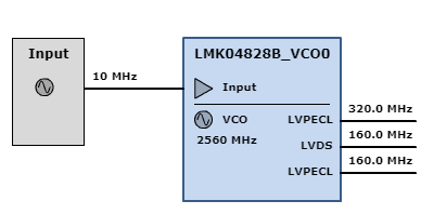
So the DAC needs a CLK signal (PECL) at 320 MHz and a DCLK signal (LVDS) at 160 Mhz. The ADC needs a CLK_IN signal (LVPECL) at 160 MHz (perhaps 320 Mhz, i am not sure).

Can I combine that somehow? not that I am very limited on connections. Due to the amound of data I only have 2 differential pairs through an FMC for the clocks.

I have combed through the data sheets but I am so confused. I hope you can help me with the design.

Should I use the same 160 MHz signal and just convert between LVDS and LVPECL or can I use the same signal for both? (the data sheet says that LVDS clock is not recommended for the ADC)

Is there a simple clock generator that only needs a 320 MHz input frequency and then output the mentioned frequencys and signal types?

Regards
Michelle

  • Hi Michelle,

    I would recommend using an LMK04828 type device. www.ti.com/.../LMK04828

    You can provide an input (from the FPGA in your case), then have many buffered outputs of different types (LVDS, LVPECL, etc...) that can be divided down. This might also be a good idea since the clock signal coming from the FPGA might not be very clean.

    Best Regards,

    Dan
  • Hi Dan

    Thank you so much for your reply.

    I have now looked at the data sheet and it does not seem as simple as I had hoped, but that might just be because I am not very experienced.

    I have looked at the CDCM7005 as well, and that seems to make more sence to me, due to the schematic of the DAC evaluation board.  Can I use that instead? 

    The programming is not an issue at the moment, but I really need help setting up the connections.

    If I go with the lmk04828 do I need an external VCO? I used TI's webench which looks very simple. It suggests a ref clk at 10 MHz and an internal  VCO at 2560 MHz, can that frequency be achieved?

    There are a lot of input clock pins,  (CLKin1, CLKin1* etc) which one do I connect the 10 MHz to, and does the 10 MHz come from the FPGA?

    how about the SDCLK_out, do I need those for the DAC and ADC?

    Regards
    Michelle

  • Depends on reference performance and ADC/DAC clock jitter requirements.
    If reference is noisy (from FPGA or recovered from PHY/SerDes), we need dual PLL jitter cleaner LMK04133 (5 pairs of outputs)/ LMK04803 (12 pairs of outputs)/LMK04828 (14 pairs of outputs, support JESD204B).
    If the reference is from a local XO, jitter performance is good enough, then we could consider single PLL devices, LMK03806, CDCM6208.