This thread has been locked.

If you have a related question, please click the "Ask a related question" button in the top right corner. The newly created question will be automatically linked to this question.

ADC121C021: information regarding malfunction of sensing circuit using ADC121C021

Part Number: ADC121C021

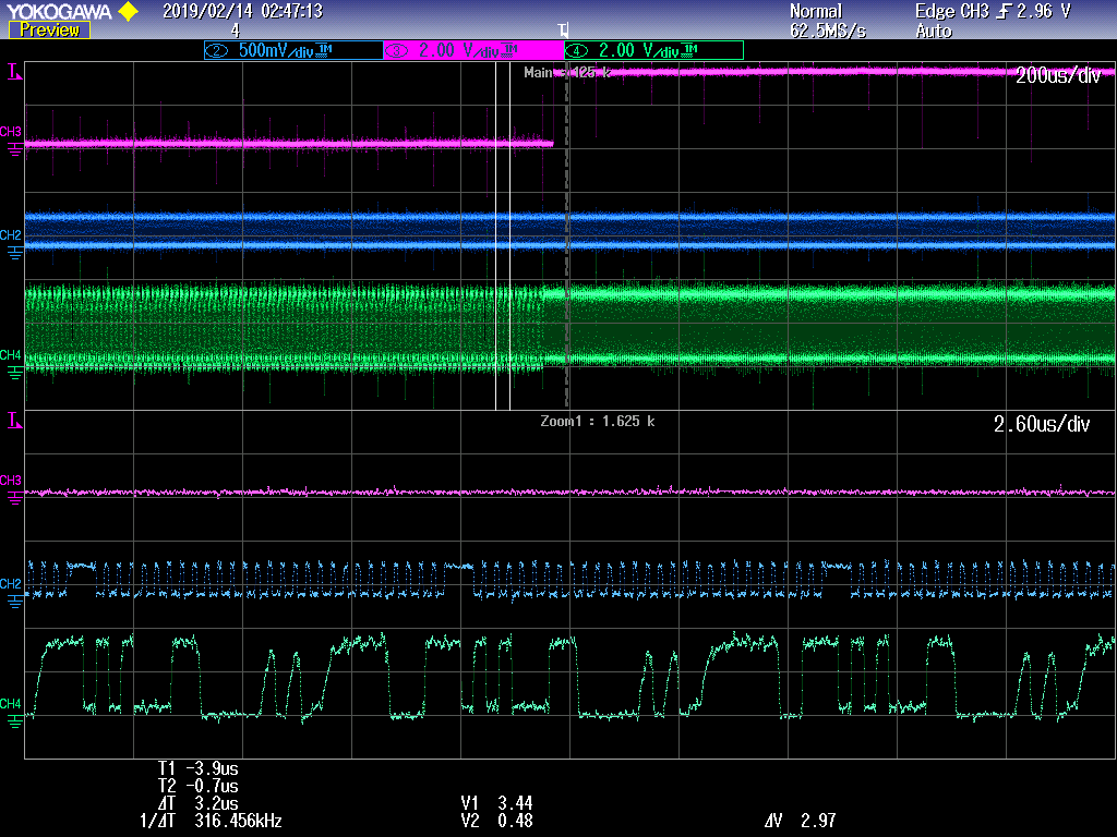
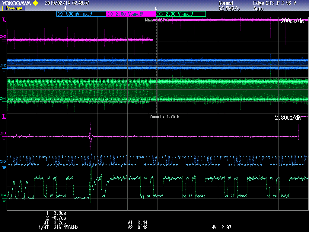
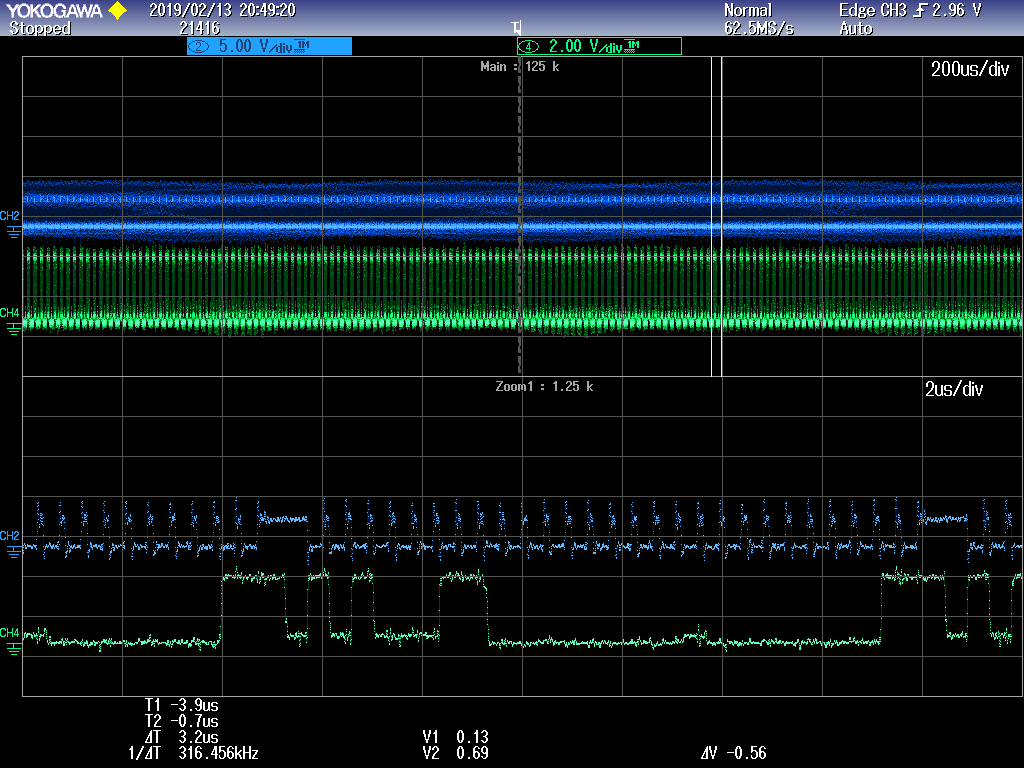
I am using  ADC121C021 which uses the I2C protocol for transferring the digital data. I am using eight of them to measure eight capacitor voltages in a power electronics circuit. Each of the eight ADCs is assigned eight different hardware addresses. According to the I2C protocol, an ADC transfers the digital data when the address on the SDA line matches with its corresponding hardware address. If it does not match, it generates a Not Acknowledgement (NACK).

Now, I am facing the following problems:
1) During some instants, the ADC generates NACK even though the address on the SDA line matches with its hardware address. The problem persists even after multiple attempts of REPEATED START.
2) The first four bits of the 16 bit digital data that ADC121C021 sends are supposed to be zero for the Non automatic mode of operation. However there are instants when the ADC sends ONEs in the first four bits.
3) There are instants where the ADC sends all 16 bits as zeros.
All these cases are interrupting the objective of sensing the capacitor voltages. Please note that there is electrical isolation provided between the high voltage capacitor voltage side and the sensing circuitry.
 I will be really grateful if someone can point out the possible reason for the problems mentioned above. 
Thanking you.
  • Hello,

    To make sure that your timing and digital communications is correct i would suggest connecting a scope to your digital lines. This will work as a visible check to confirm that what is expected on the figital lines is what the devices are seeing. Please share scope shots. Have you tried testing one device at a time, without any of the other 8 connected to the bus? Once you have correct communication with one device, you can add the other devices.
  • Thank you for your response.

    Yes I have tried communicating with one ADC at a time.

    The SCL frequency is kept to be at 3.3 MHz with 100ns as the High time and 200 ns as the Low time. 

    In the figures below, Ch-2 is the SCL and Ch-4 is the SDA.

    The image below shows the status of the data lines when the communication is happening. The slave address is 51H

    The image below shows the transition from the working mode to the case when the ADC sends NACK. The ADC continues to send NACK even after continuous attempts of Repeated Start.

    The image below shows the case when the ADC sends all bits as zeros.

    The image below shows the case when the ADC sends all bits as ones.

    These problems were not observed when the ADC was operated in 100 kHz. with equal High and Low times (i.e. 5 microseconds each).

    The ADC is again operated with a SCL period of 440 ns with 120 ns as the High time and 320 ns as the Low time. This unequal low and high times are chosen based on the following information given on PAGE 8 of the datasheet. 

    The behaviour of the ADC when it enters the NACK zone is a bit different in this case as shown in the image below. After the slave address of 51H, Write bit is given and then the ADC sends NACK. The subsequent bit is supposed to be One according to our code. This was the case in 3.3 MHz operation. However, in the image below you can see a dip in the Bus voltage, which we are not able to explain. This is followed by the repeated start.

    The capacitor voltage sensing circuit consists of a potential divider to step down the capacitor voltage to the level of the IC voltage. This is followed by an isolation amplifier stage. The output of the isolation amplifier is a differential type where as the ADC is single ended. So a differential amplifier is used to connect the isolation amplifier with the single ended ADC. The cut off frequency of the differential amplifier is around 10 kHz. 

  • Thank you for providing the scope shots. They are rather difficult to read though, as there is a lot of noise, in some cases there are large spikes. I would suggest cleaning this up, the noise could be greatly affecting your I2C communication. You mentioned you are measuring power scheme, you need to make sure that power line noise is not affecting your digital lines. In your layout it is good practice to keep your digital signals far and separate from your analog signals. Also, can you try slowing down your communication, this could help clearly see any timing issues.

    From looking at your scope shots, it might be possible that the timing requirements are not being met. It is not too clear, but seems that SDA and the falling edge of SCL are almost in-sync. It is best to make sure that SDA engulfs the entirety of the SCL pulse. See Data Hold Time timing requirement; I am assuming you are using High speed Mode with Cb = 100pF, this means that you need a minimum of 70nS hold time between falling edge of SCL until SDA should change states.

    Regards
    Cynthia