Because of the holidays, TI E2E™ design support forum responses will be delayed from Dec. 25 through Jan. 2. Thank you for your patience.

This thread has been locked.

If you have a related question, please click the "Ask a related question" button in the top right corner. The newly created question will be automatically linked to this question.

DAC161P997: DAC161P997 communication issue

Part Number: DAC161P997
Other Parts Discussed in Thread: DAC161S997, LM2936

Hello experts,

I have a custom PCB designed based on the DAC161P997 evaluation board, currently the DAC doesn't respond to the bit stream I am sending. I can't see any ACK response or the ERRB pin signal being lowered by the device. According to the section(and from the settings R210 DNP) the default error current should be around 3.3mA but the I can read a fixed loop current of 14.8mA. I might be missing something in the hardware which I can't seem to find. Schematic is attached for the reference and any help here is appreciated.

-Muneeb2821.Schematic.pdf

  • Hello,

    Is the loop current stable at 14.8mA DC or is it toggling? Can you provide a scope capture of DIN when you are sending the data? Also, what voltage do you measure on the ERRB pin?

    Thanks,
    Garrett

  • Hi Garrett,  Thank you for your quick response.

    1. Yes the loop current is stable at 14.8mA

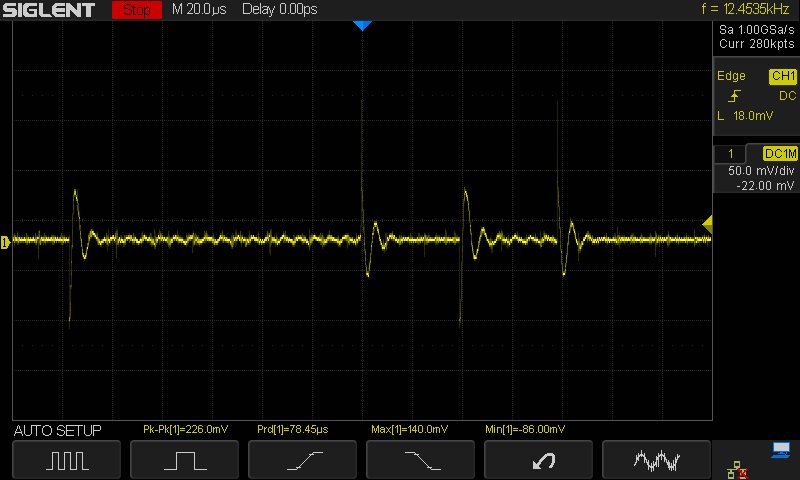
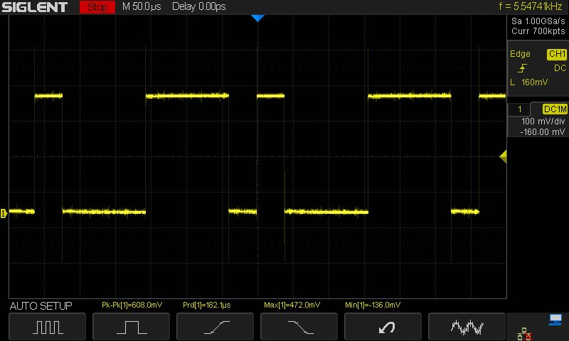
    2. Scope shot of the transmission is attached before and after the transformer.

    3. ERRB pin is at 3.9V.

    Let me know if you need more information on this.

    -Muneeb

  • Hi Garrett,

    Can you confirm the waveform at the signal transformer is correct?

    -Muneeb

  • I'm looking for a solution to this same problem. was there a solution for it?
  • Hi Muneeb,

    1. The device should regulate the loop current to ERRLOW (3.2mA) by default since you have ERRLVL tied low. This means that the circuit is not correctly regulating the loop current. I notice you use both GND and COM in your design. How are these related? In loop powered devices all devices on the board should be referenced to COM of DAC161S997.

    2. It does not look correct on the secondary side of the transformer.

    3. ERRB is an open drain pin that is pulled up to 3V3. How can this be 3.9V? What is the voltage measured at the output of the regulator LM2936?

    Thanks,
    Garrett
  • Hi Garrett,

    Thank You for your response, The GND and COM were intended to use the system power or external power as loop power which I believe have some issues. For now I have disabled this and reference is COM for all circuitry now. The ERRB pin voltages were measured with reference to GND and voltages at LM2936 with reference to COM were and are at 3.3V. After referencing through COM I have following findings.

    1. ERRB pin is now at COM potential means error condition is asserted.
    2. Loop current is not regulated at 3.3mA but swinging between 15-20mA.

    Is there any other suggestion to check what is causing error current to this value? I am sorry I don't have the evaluation kit as a reference and relying on your input and which is highly appreciated.

    Thanks
    -Muneeb

  • Hello Muneeb,

    1. It is not surprising that ERRB is low as the 'CHANNEL' error reporting is enabled by default. So if the device receives no communication over a period of time ERRB will be asserted low and the loop current should go to ERRLOW to report this error.

    2. It is strange that the loop current is toggling but as you stated earlier ERRB is not. Can you provide a scope capture of the loop current or voltage across your load resistor?

    I would focus first on getting the device to regulate the loop current to ERRB before doing any debug with your communication. If it is not regulating the loop current correctly in the first place there is no need to analyze the SWIF waveforms.

    Can you also show how you are connecting your load and power supply? I believe R207 should be connected in series with pin 8 of LM2936 before C109. I don't think this is the cause of the problem but it does sacrifice headroom for the current loop.

    Thanks,
    Garrett
  • Hi Garrett,

    I can feel the abnormal heating at the DAC IC and suspecting something is really bad, my assembler does have history of ruining boards. I will assemble an isolated(alot of circuitry is there on the board) section over the weekend on new board and will let you know all the captures you asked for. Plus I noticed the R207 issue and I will put that in series to the LM2936. 

    Regards
    Muneeb

  • Hi Muneeb,

    Alright, let me know when you have an update.

    Thanks,
    Garrett
  • Hi Garrett,

    Hope you are doing well. I had assembled the minimal circuit on a separate board and now the ERROR current is regulating to expected value and that's a positive thing. Currently I haven't assembled the isolation transformer and directly coupling the DIN and ACK pins to the MCU. I am trying to write DACCODE 0x2AAA (4mA) but I can't see the out current changing or any ACK feedback on the ACK pin (I have the pull up resistor added). Here is the capture of a single frame I am sending, can you please take a quick look on the frame if there are correct specifically the parity bits.

    In addition to this can you let me know if it's necessary to write configurations registers first or I can directly write to DACCODE?

    Thanks
    -Muneeb

  • Hi Muneeb,

    Glad you got the device regulating the current correctly.

    Your frame looks okay for 0x2AAA to the DACCODE register. Your parity bits look okay as well:

    P0 = [(# of ones in LOW Slice(4)) mod 2 ==0] = 1

    P1 = [(# of ones in HIGH Slice(3)) mod 2 ==0] = 0

    You should be able to write to DACCODE without writing to the config registers first. The config registers are locked by default. What is the voltage level of the above logic waveform? Could you share the schematic of your 'minimal' circuit?

    Thanks,
    Garrett
  • Minimal circuit.pdf

    Hi Garrett,

    The voltage level is 3V, I am powering DAC from ST's development board which have on board 3V regulator. I am sure 3V are withing limits to DAC (2.7~3.6V). The schematic is attached for the reference, loop is powered with a 12V power supply with an ammeter connected in loop. The ACK pin also have pull up connected.

    -Muneeb

  • Hi Muneeb,

    Sorry, but I am a little unclear of the DNP components. I understand you are directly interfacing with the SWIF with an MCU but it doesn't appear ACKB is connected, assuming the DNP labels are correct. In this case you will not see an acknowledge response unless you mointor ACKB separately. ACKB will need a pull-up resistor as it is open drain.

    Do you see the loop current change when you send the frame?

    Thanks,
    Garrett
  • Hi!

    I was afraid you might get confused. DNP parts are not mounted on the board but as I mentioned in my previous replay the ACKB pin does have pull up connected to the 3V power supply. The DIN and ACKB pins are connected to two separate GPIOs of the MCU with ACKB having pull up resistor.

    I either can't see anything on ACKB pin(a LOW level) and nothing is changing in the loop current, it's stable at 3.23mA while I am sending the frames. I tried lowering the frame rate as well but still nothing. Is there anything else I can provide you to analyze the issue? May be scope picture of both DIN and ACKB pins?

    -Muneeb

  • Hi Muneeb,

    Thanks, I understand now. It would certainly be helpful if you provided scope shots of DIN and ACKB. Your frame looked okay on the logic analyzer but it would be better to see the waveform on the device pins. That's my main suspicion that something could be distorting the frame.

    Thanks,
    Garrett
  • Hi Garrett,

    The scope capture of both DIN and ACKB pins are attached. Let me know if these looks good or you spot any issue. The capture is not of a full frame but I am assuming these are enough to give you hint of the voltages levels of the frame.

    -Muneeb
    Scope_Capture_ACKB_DIN.pdf

  • Hi Muneeb,

    Thanks for providing the scope captures. I think the issue is the waveform has a DC offset and a small amplitude for some reason. From your scope capture the amplitude appears to be +/-500mV with an offset of 2V. This means that it never transitions below VIL and is not seen by the digital interface. What is the reason for the DC offset?

    Thanks,
    Garrett

  • Hi Muneeb,

    Any update on this?

    Thanks,
    Garrett
  • Hi Garrett,

    Thank You for the help, as I was working with the existing board and connections to the MCU were done through wires for test purposes and there was an invisible strand of wire shorting DIN line to 3.0V and that was causing the offset. As this is fixed the communication worked fine and so the output current. I am also soldering the isolation circuitry and going to check the communication with that. If it works fine I will mark the post as resolved else I would need a little more help of you. Thank You again for pointing the issue.

    Regards
    Muneeb Khan

  • scope_capture_isolation.pdf

    Hi Garrett,

    Here is update, please check the attached scope captures at various points(3.0V MCU is replaced with 3.3V). With isolation circuitry added the DAC does regulate fine to error current but doesn't recognizes the frame. The frame voltages reaching at DIN pin are too low for the DAC logic. The same frame does work fine when directly coupled to DIN and MCU pins.

    Can you please verify the buffer configuration in the schematic?

    -Muneeb

  • Hi Muneeb,

    Glad you got it working with the direct interface, that is good progress.

    The waveform is not correct. It should be a damped impulse response. For the buffer configuration it looks like you mixed the Figure under heading 8.2 and Figure 28 application circuits in the datasheet. Which one are you trying to implement?

    Thanks,
    Garrett
  • Hey Garrett

    i'm posting on behalf of muneeb since he is unable to access his computer right now. This is his feedback:

    "I am implementing Figure 28 with single rx/tx pin and rx_tx_en pin. The DC blocking circuit is straight forward but still it’s not working as expected. Can you suggest any debugging points here?’

    Please still feel free to address muneeb 

    Thanks

    Travis

  • Hello,

    I would recommend implementing the circuit shown in Figure 30 first to make sure your isolation circuit is working. Note the direction of current flow in the isolation transformer shown in Figure 30. It is opposite of your configuration.

    Thanks,
    Garrett
  • Hi Garrett,

    Thank You for your suggestion but with the current board it's hard to test this way. We may need to go for an iteration of the board. I have question and that probably be the concluding question of the ticket. I have implemented Figure 31 with digital isolator between the MCU, DIN and ACKB pin. It's working fine and I think we can go this way without further investing time on this issue. Let me know if I am missing something with use of digital isolators with reference to Figure 31. If everything is good this way, we are closing this ticket with many thanks for your help and patience.

    Regards
    Muneeb Khan
  • Hi Muneeb,

    You can use a digital isolator if it is okay in your application. Typically digital isolators will draw more current than the transformer configuration.

    Thanks,
    Garrett
  • Hi Garrett,

    Thank You for the help, I have marked the reply that resolved my issue.

    Regards
    Muneeb Khan
  • Hello Muneeb,

    Glad to assist in resolving your issue. Feel free to post again if you run into anymore issues with the DAC.

    Thanks,
    Garrett