This thread has been locked.

If you have a related question, please click the "Ask a related question" button in the top right corner. The newly created question will be automatically linked to this question.

ADS8695: SPI example code for ADS8695

Part Number: ADS8695
Other Parts Discussed in Thread: ADS8681

Dear

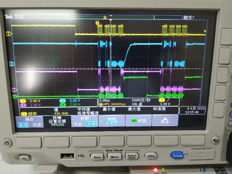
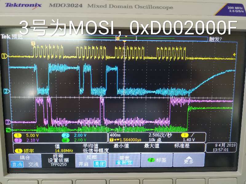
Customer ask whether we have SPI example code for ADS8695 can be their reference? Thanks.

They meet a issue that whatever they set the ADS8695 register value, the read sample value always base on the default register setting.

  • Hi Terry,

    Unfortunately we do not have example code for this device, can you please provide more information?

    1. The commands with the data to program and read the register, which register is the customer trying to program and read?

    2.  Timing plot for SCLK/SDI/SDO and CONVST/CS will be very helpful to address the issue, the timing for one frame and two continuous frames will be great.

    Thanks&regards

    Dale

  • Hi Dale

    Below is waveform example, we try to send "program register" command then send "read register" command. 

    The "program register" command is 11010000-00000010-00000000-0000FFFF

    and "read register" command is 11001000 - 00000010 - 00000000 - 00000000

    no matter how many times to send "read register" command, the feedback is not register data, but always ADC sample result data base on default register setting.

    could you please help check if anything we operation wrong?

  • Hi Terry,
    These commands are correct if the customer is trying to program DEVICE_ADDR[3:0] in DEVICE_ID_REG register and read it back. Please note that the register data will be shown in next frame, not same frame as sending Read_HWORD command. Is Blue timing for SDO from ADC? Was this data on SDO all same in different frames?
    Looks like the customer is using SPI-00 protocol which is correct because the ADC supports this protocol for data read and write operations after power up. However, there are few things in the timings made me confused:
    1. In first timing graph, there is one change from high to low on SCLK and MOSI, is this the first frame after configure the SPI on the customer's CPU?
    2. The initial signal level on MOSI between 2nd and 3rd timing graph is different, was anything changed?
    Without programming any internal registers, was the conversion data correct regarding the analog input signal? this can demonstrate if the SPI timing is correct.
    We can have a call if you want.

    Thanks&regards,
    Dale
  • Hi Dale

    Yes, we are testing the commands to program DEVICE_ADDR[3:0] in DEVICE_ID_REG register and read it back. If our command is correct, then what continue command or data we should send to get the correct register data feedback in next frame? 

    And Blue timing is SDO from ADC, so far no matter how many times we send Read_HWORD by continue, the SDO always return conversion data which is correct according analog input signal and we also can succeed receive the conversion data in SPI Rx Buf.

    Regard your question:

    1, Yes, the first timing graph is the first frame after configure SPI so you can see the high to low on SCLK and MOSI

    2, We donot change anything between 2nd and 3rd timing graph, the different maybe cause by last MOSI byte in 2nd graph is "0F" and in 3rd graph is "00"  

  • Hi Terry,

    Thank you for clarification.

    If the READ_HWORD command is sent to ADC in frame F,the same command or a NOP command can be sent to ADC in frame (F+1), and the output data word in frame (F+1) contains 16-bit register data and followed by 0's. Please make sure to use CONVST/CS signal because the command will get executed at the rising edge of the CONVST/CS signal. See the description on page 41 and 42 of ADS8695 datasheet.

    Thanks&regards,

    Dale

  • Hi Dale

    Yes, we have read the page 41/42 and try to send command follow our understand as below:

    CS falling to LOW -> WRITE HWORD -> CS rising to HIGH -> CS falling to LOW -> READ HWORD -> CS rising to HIGH -> CS falling to LOW -> READ HWORD -> CS rising to HIGH

    We suppose to see register value back on 2nd READ HWORD frame, however it is always the conversion data in all above three frame. 

    Do we understand wrong for the Command and CS signal operation?  Or do you think anything others setting we are missing in here? 

  • Hi Terry,
    I did not see something was wrong with your CS signal, I'm trying to double check and may setup a bench with a software to check, it will take few days, thanks for patience.

    Best regards,
    Dale
  • Hi Terry,

    Let's focus on Reading the register firstly then we can check register programming later. Can you ask the customer to send the commands as below and capture the timing plot(/CS,CLK,SDI and SDO) for two frames(32 clocks+32 clocks)?

    1. Send command( 0xC8240000)  to ADC o read ALARM_H_TH_REG Register.

    2. Send NOP command (0x00000000) with 32 clocks to ADC.

    Remark:  the reason we read ALARM_H_TH_REG Register is the default content in this register is 0xFFFF at bit 15-0. Hence, 0xFFFF should be observed on SDO in first 16 bit in 2nd frame.

    Please refer to another query that has the latest timing plot the customer got on reading register from ADS8681.

    https://e2e.ti.com/support/data-converters/f/73/t/790523

    Thanks.

    Regards,

    Dale