This thread has been locked.

If you have a related question, please click the "Ask a related question" button in the top right corner. The newly created question will be automatically linked to this question.

DAC7678EVM: Reading output voltages on DAC7678

Part Number: DAC7678EVM
Other Parts Discussed in Thread: TMS320F28377S,

I'm interfacing with the DAC7678EVM using a TMS320F28377S as the I2C master controller. I am writing a sequence of bytes to power up the DAC Channel and write a value to it

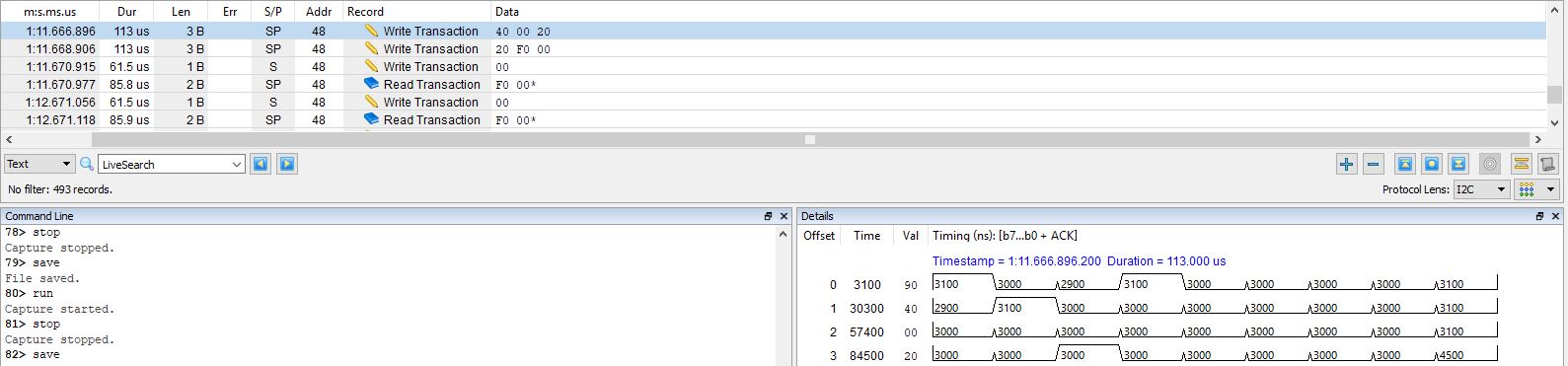
DAC Slave address: 0x48

Power up Command and Access Byte: 0x40

Data Bytes: MSB: 0x00  LSB: 0x20      (Power up DAC channel A)

Write Command and Access Byte: 0x30   (Write to DAC Channel A and update individual Channel)

Data Bytes: MSB: 0xF0  LSB: 0x00  (Value should correspond to 3.840 V)

The multimeter reading shows 3.842 V as expected on DAC Channel A (J1.2) however, all other DAC channels are set at about a mid-scale reading of 2.05 V

I changed this second sequence to

Write Command and Access Byte: 0x20   (Write to DAC Channel A and update all channels)

Data Bytes: MSB: 0xF0  LSB: 0x00  (Value should correspond to 3.840 V)

I got the same readings on the multimeter. Is this behavior expected? I'm not sure of why all the other channel outputs show 2.05V

  • Hi Ruta,

    Thank you for your query. Could you please upload scope shots of the i2C pattern?

    Regards,
    Uttam Sahu
    Applications Engineer, Precision DACs
  • Hi Uttam, thanks for your reply.

    I am using a protocol analyzer to monitor the I2C pattern.  Here are the images:

    1. Power up DAC Channel A Sequence (See timing data)

    2. Write Voltage level (0xF0 = approx 3.840V) to Channel A and update Channel A (Individual software LDAC)

    3. Power up Channel A (same pattern as 1)

    4. Write Voltage (0xF0 = 3.840V) to Channel A and update all channels (global software LDAC Command/Access byte)

    Is there something wrong with the power-up/write/update pattern? I can see the correct voltage on Channel A analog output (Pin J1.2 on the DAC7678EVM)  however all the other channels B-G show 2.050V output.

    In that case is there a specific power up and update sequence that is expected?

    Thanks.

  • Noted the configuration of RSTSEL pin on EVM which was floating.