This thread has been locked.

If you have a related question, please click the "Ask a related question" button in the top right corner. The newly created question will be automatically linked to this question.

AFE5828: 12-bit ADC issue

Part Number: AFE5828
Other Parts Discussed in Thread: AFE58JD28

Hi, there

I am using AFE5828 in our project to collect data. The AFE5828 ADC is configured to 12-bit. The PGA clamp level is set to 1.26Vpp; the LNA gain 21 dB; and the PGA gain 27 dB.

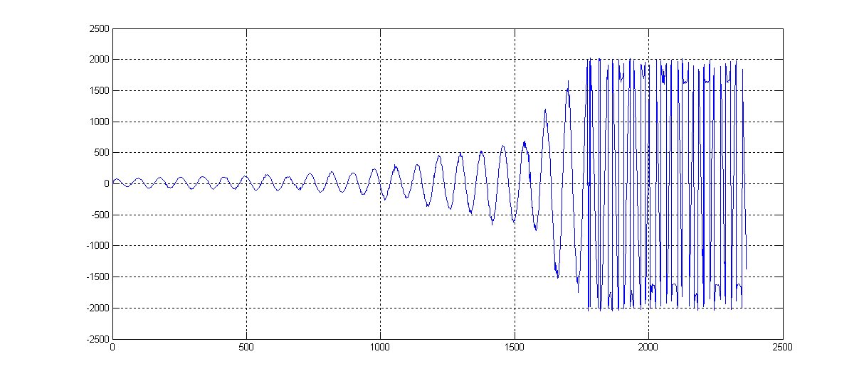
I did a test by applying a sine wave signal to the input. The collected data is plotted as follows:

The data is interpreted as signed value. The Voltage Control Attenuation is reduced with time from 36dB to 0dB.

I got a doubt on this set of data: Why does the data value flip the sign when the amplitude keeps increasing? How to work around this issue? Did I miss any thing?

Looking forward to your reply.


Sincerely


FENG WU

________________________________________________________________________

Feng Wu, Ph.D.
LinkQuest Inc.
6749 Top Gun Street, Suite 100
San Diego, CA 92121
Tel: (858)623-9900, 623-9916 ext. 103
Fax: (858)623-9918
Email: fwu@link-quest.com
www.link-quest.com/sq
www.link-quest.com

  • Feng,

    Thanks for using the AFE5828!

    Did you set the ADC format as offset binary or 2's complement? Please run a RAMP test pattern to make sure the FPGA capture is good.

    please also change the PGA clamp to other settings and see whether this helps. when it clamps, it will cut off the tops.

    Thanks!
  • Sean,

    Thanks for your reply.

    1) I did a test by setting the 5828 to output a ramp pattern. It went well, the collected data is a perfect ramp. So, my FPGA works good.

    2)  I tried all 4 clamp levels instructed in the manual. The output is clamped at different value (of course, flipped).

    3) I did not find any place to set the ADC output format. By looking at the received data, I think the ADC output format (for the sine-wave input) is the 2's complement. So I interpreted the data accordingly. As shown in the figure, the 2's complement format works good when the signal's amplitude is small ( the absolute value lower than 2047). It only failed when the amplitude keeps increasing beyond the 2048. 

    It looks like that the ADC output is always represented in 14-bit 2's complement format. The 12-bit output is not from the MSB. The sign bit is discarded. Based on this theory, all the data would be explained.

    Looking forward to your further guidance

    Thanks

    Feng

  • the default ADC output is LSB first. Reg.4[4] is to set that. hope this solves your issue.

    Thanks!

    Xiaochen
  • Sean,

    I did set the Reg4[4] to 0 as LSB first, and Reg4[1-0]  00 as 12-bit resolution.

    Thanks

    Feng

  • Feng,

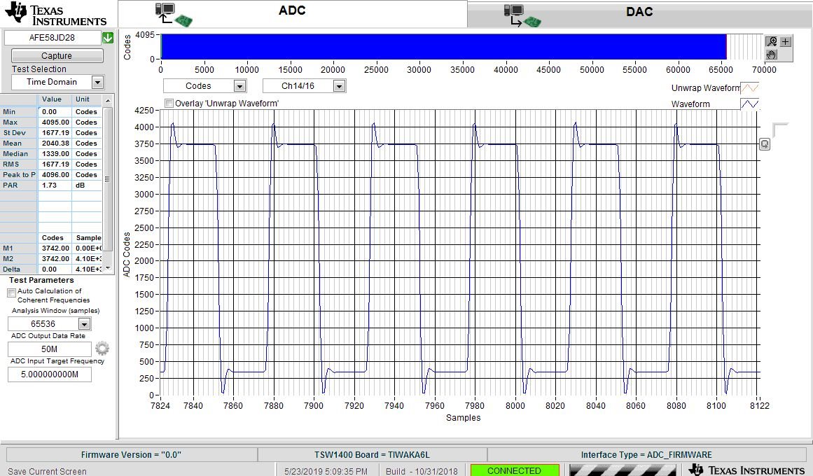
    our lab results shows correct clamp settings. please take a look.i feel you might need to look at the decoding int he FPGA. what we did is

    Data Postprocessing=1:2048

    \\1=xor, i.e. input xor.2048 to get the ADC data.

    Thanks!

  • Hi, Sean

    Thank for your prompt reply.

    I'll check my FPGA code again, and let you know when I'm done.

    Thanks
  • Hi, Sean

    I checked my FPGA by setting a custom value and ramp signal, it works well. No problem with my FPGA.

    I interpreted the data the same way as yours, i.e. input xor.2048 to get the ADC data. So the interpretation is ok.

    For AFE5828 ADC working at 12-bit, I suspects there are some settings I did not make them right.

    Would you mind checking the settings for me at your convenient time?

    The settings I used:

    ; reset
    reg 0 : 0x0011

    ; set clamp level 010 : 1.26 Vpp clamp
    reg dd : 0x0000
    reg c6 : 0x4000

    ; set all registers with 1
    reg 01 : 0x0014
    reg 03 : 0x0010
    reg c5 : 0x4000
    reg d0 : 0x0001
    reg de : 0x00c3
    reg df : 0x0040

    ; pll
    reg 41 : 0x8000
    reg 42 : 0x8000
    reg 41 : 0x0000
    reg 42 : 0x0000


    Tx_Trig Pulse

    ; GAIN PGA = 27 dB, LNA = 21 dB, LPF : 10MHz
    reg c5 : 0x6002
    reg d0: 0x0005

    ; Disable digital features
    reg 02: 0x1000

    ; 12-bit resolution, LSB first
    reg 04: 0x0000


    Thanks a lot

    Feng
  • Feng, 

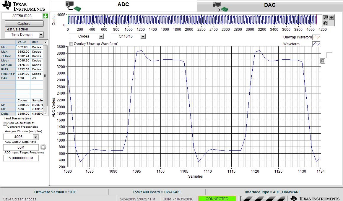
    i run the below . look like the capture is still OK.  the only difference is that i enable the digital DTGC for Max gain at the end. i don't think it matters to your flipping case. 

    can you please try to use digital TGC and match my setting exactly. i input a 2MHz 100mVpp signal from fun generator. if digital is no problem, we need to look at your TGC control path. 

    Thanks!

    AFE58JD28_ADC|0x00 0x0011
    AFE58JD28_VCA|0xDD 0x0000
    AFE58JD28_VCA|0xC6 0x4000
    AFE58JD28_ADC|0x01 0x0014
    AFE58JD28_ADC|0x03 0x0010
    AFE58JD28_VCA|0xC5 0x4000
    AFE58JD28_VCA|0xD0 0x0001
    AFE58JD28_VCA|0xDE 0x00C3
    AFE58JD28_VCA|0xDF 0x0040
    AFE58JD28_ADC|0x41 0x8000
    AFE58JD28_ADC|0x42 0x8000
    AFE58JD28_ADC|0x41 0x0000
    AFE58JD28_ADC|0x42 0x0000
    AFE58JD28_ADC|0x04 0x0000
    AFE58JD28_ADC|0x41 0x0002
    AFE58JD28_VCA|0xC5 0x6002
    AFE58JD28_VCA|0xD0 0x0005
    AFE58JD28_ADC|0x04 0x0000

    AFE58JD28_VCA|0xCE 0x8000

  • Hi, Sean

    I tested your setting. It did not solve my problem.

    I did some analysis on my collected data. I found that the sign bit (bit 11) of each previous sample is grouped into the next sample as lowest bit (bit 0). This one bit shift could explain my collected data well for the 12-bit LSB first output. For example, all the consecutive positive numbers is even number; all the consecutive negative numbers are odd number; and most important, the signal curve is not flipped.

    Looks like the data is not collected correctly, however, as I told you, there is no any error found for collecting the pattern data. 

    What am I missing ?

    Feng

  • Hi, Sean

    I solve it.

    You're right. The problem is the FPGA logic. When I set the custom value, say, b1111,1111,1110, and LSB first, I should look for b0111,1111,1111, instead of b1111,1111,1110.

    Thank you so much for your help.

    Feng